Method for epitaxially growing ultrathin organic crystalline layers on surface and its applications

An epitaxial growth, organic semiconductor technology, applied in the direction of crystal growth, single crystal growth, single crystal growth, etc., can solve the problems of poor crystal quality of organic materials, unsuitable for LED displays, difficulties in ultra-thin organic semiconductors, etc., to achieve high quality. Effect

Active Publication Date: 2017-08-29
NANJING UNIV
View PDF3 Cites 12 Cited by
  • Summary
  • Abstract
  • Description
  • Claims
  • Application Information

AI Technical Summary

Problems solved by technology

First, the growth of organic materials is uncontrollable and the quality of the crystals formed is poor. This process forms many grain boundaries on the organic film.
Second, the thickness of organic crystals is very large (normally hundreds of nanometers), making the fabricated devices opaque and unsuitable for LED displays
But similar to the case of graphene, low-cost, simple, and large-scale preparation of ultrathin organic semiconductors on hBN substrates for electronic applications remains difficult.

Method used


Image

  • Method for epitaxially growing ultrathin organic crystalline layers on surface and its applications
  • Method for epitaxially growing ultrathin organic crystalline layers on surface and its applications
  • Method for epitaxially growing ultrathin organic crystalline layers on surface and its applications

Examples


example 1

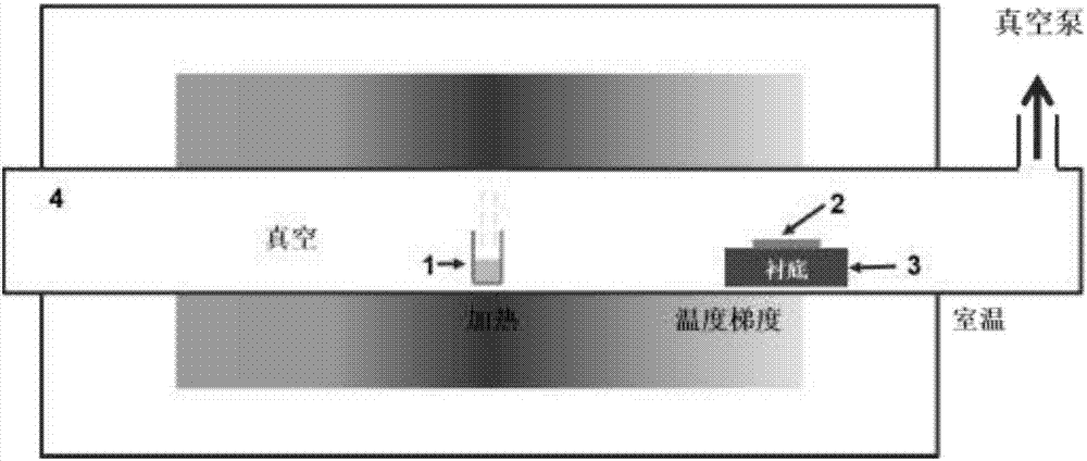
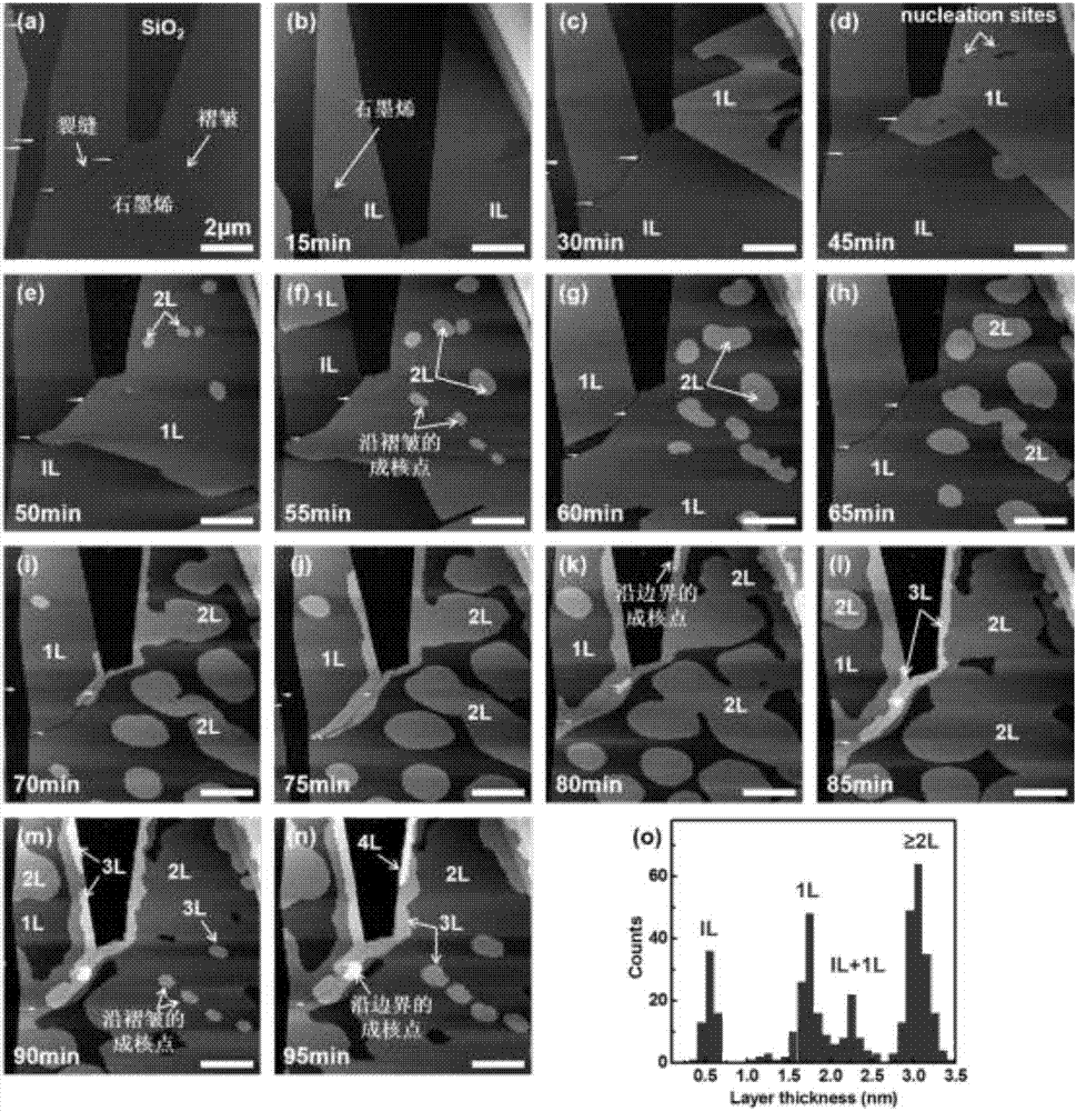
[0100] Example 1 Growth of C8-BTBT crystals on graphene

[0101] To prepare surface area up to 500um 2 Graphene samples on 285nm SiO 2 / Si substrate exfoliated graphene samples without heat treatment. The exfoliated graphene before growth was characterized by optical microscopy, AFM, and Raman spectroscopy to obtain thickness and morphology information. Growth in figure 1 In the tube furnace shown, in the tube furnace, an open container containing C8-BTBT powder (taken from Nippon KAYAKU Co., Ltd. without further purification) was placed in a quartz tube cavity (1.5 m long, 10cm in diameter). Then place the graphene sample at a distance of 20um from the source, seal the chamber of the quartz tube and evacuate it to 4x10 by a turbomolecular pump -6 Torr. For excellent reproducibility, the separation between the source and the graphene sample must be accurately measured for each experiment. The C8-BTBT powder was heated to 100 °C to start growth, after 50 min of growth, t...

example 2

[0102] Example 2: Using the same method as Example 1, except changing the distance between the source and the substrate to 10cm to grow C8-BTBT crystals, as a result, about 3 layers of C8-BTBT crystals will be epitaxial on graphene.

example 3

[0103] Example 3: Using the same method as Example 1, except changing the distance between the source and the substrate to 25cm to grow C8-BTBT crystals, as a result, about 2 layers of C8-BTBT crystals will be epitaxial on graphene.


PUM

PropertyMeasurementUnit
thicknessaaaaaaaaaa
thicknessaaaaaaaaaa
thicknessaaaaaaaaaa

Abstract

Disclosed is a method for depositing ultrathin layers of an organic semiconductor material on a support, and its applications in fabrication of electronic devices like OEFT and diodes. In the method, a source of an organic semiconductor material and a support are spaced from each other in a vacuum chamber and subjected to a temperature gradient, and the epitaxy initiates due to a van der Waals interaction between the organic molecules and the support. The ultrathin crystalline layers of the organic semiconductor material can be only a-few-molecule thick and even one-molecule thick in total. Further disclosed is a layered structure produced by said method and use of the layered structure in fabrication of logic gates.

Description

technical field [0001] The invention relates to a method for growing a two-dimensional (2D) layered heterojunction, specifically a method for epitaxially growing an ultra-thin organic semiconductor crystal layer on the surface of graphene and hexagonal boron nitride (hBN), and its Applications in the fabrication of organic thin film transistors (OFETs) electronic devices. Background technique [0002] Two-dimensional layered organic crystalline materials are promising materials for applications in electronics and optoelectronics. Compared with bulk materials, single-layer crystals can effectively reduce the interlayer shielding, so it can provide an ideal system for directly studying the influence of grain boundaries and interfaces on charge transport, and the carrier injection and modulation become more efficient, which can greatly to improve the performance of OFETs. [0003] OFETs are important components of drive circuits for flexible, low-cost, portable electronic app...

Claims


Application Information

Patent Timeline
Patent Type & Authority Applications(China)
IPC IPC(8): C30B29/54C30B23/06
CPCC30B23/06C30B29/54C30B23/002C23C14/12H10K71/164H10K85/6576H10K10/484
Inventor 王欣然施毅李盷定光雄一滨田真弘
Owner NANJING UNIV
Why Eureka
Try Eureka