Metal metamaterial wave plate

A metamaterial and metal technology, applied in the field of metal metamaterial wave plates, can solve the problems of large structural aspect ratio, difficult preparation, and difficulty in popularization, and achieves the goal of reducing reflection and absorption loss, improving conversion efficiency, and improving integration. Effect

Inactive Publication Date: 2017-10-10
INST OF SEMICONDUCTORS - CHINESE ACAD OF SCI
View PDF6 Cites 9 Cited by
  • Summary
  • Abstract
  • Description
  • Claims
  • Application Information

AI Technical Summary

Problems solved by technology

However, most dielectric metamaterial waveplates use silicon as the working medium. Due to the limited band gap of silicon, this type of waveplate cannot maintain high efficiency in the band above 300 terahertz.
Although some devices using wide-bandgap dielectric materials such as titanium oxide can adapt to wider bands, their structural aspect ratio is too large, making preparation extremely difficult and costly, making it difficult to popularize
Wave plates based on metal metamaterials can flexibly adjust the working band of the device through the structural design of the material, but this type of wave plate uses the surface plasmon resonance of metal materials, so the loss will be relatively high
At the same time, using a single-layer metal nanostructure wave plate with a thickness smaller than the wavelength cannot effectively control the reflection loss, so the efficiency of metal metamaterial wave plates in the optical band is generally low
The use of coupling between multilayer metal metamaterials to simultaneously generate electrical resonance and magnetic resonance to form a Huygens metasurface can improve the efficiency of metal metamaterial wave plates, but the efficiency of metal metamaterial Huygens metasurfaces is still at present. Less than 50%, and its structure is complex and difficult to prepare

Method used


Image

  • Metal metamaterial wave plate
  • Metal metamaterial wave plate
  • Metal metamaterial wave plate

Examples


no. 1 example

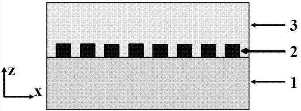
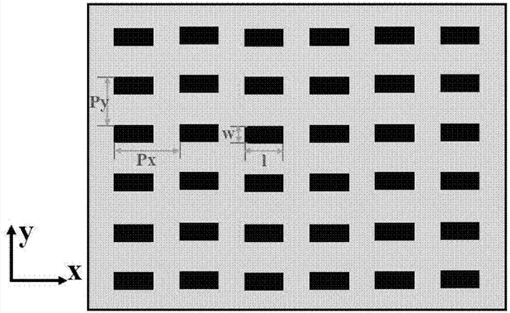
[0051] The metal metamaterial wave plate in this embodiment is a half-wave plate, which can rotate the polarization direction of incident light by 90 degrees, its working wavelength is 1.1 um, and its transmission efficiency is above 80%. The material of the dielectric substrate and the dielectric cladding layer of the half-wave plate is both quartz, and the material of the metal particles is silver. The size of the metal particle is: long axis length l=340nm, short axis length w=200nm, height h=360nm. The metal particle period along the x-axis direction is Px=600nm, and the period along the y-axis direction is Py=620nm.

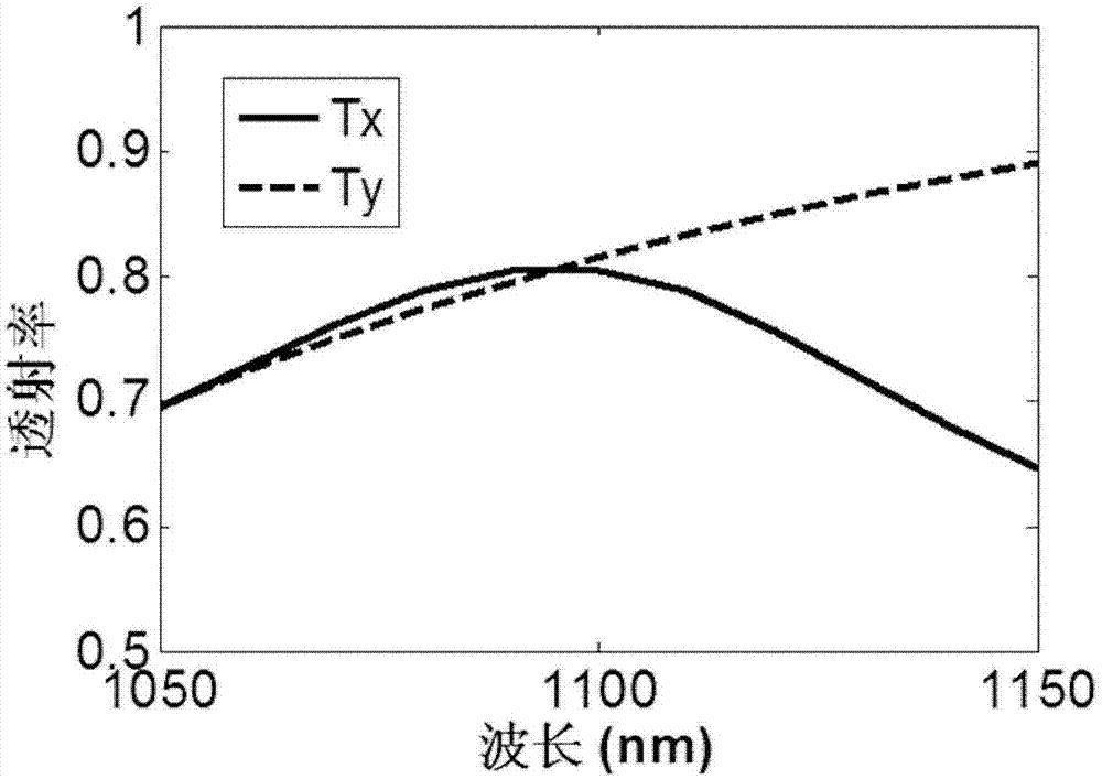
[0052] The polarization direction of the incident light forms an angle of 45 degrees with the long axis and is perpendicular to the wave plate, so the intensity of the incident light component in the direction parallel to the long axis and the short axis is the same. image 3 is the variation curve of the transmittance of the incident light component polari...


PUM

PropertyMeasurementUnit
lengthaaaaaaaaaa
lengthaaaaaaaaaa
heightaaaaaaaaaa

Abstract

The invention provides a metal metamaterial wave plate. The metal metamaterial wave plate comprises a medium substrate, a metal metamaterial layer and a medium wrapping layer, wherein the metal metamaterial layer is arranged on the medium substrate and comprises metal particles periodically arrayed; the medium wrapping layer is arranged on the metal metamaterial layer and used for providing impedance matching; the metal particles periodically arrayed are distributed in a rectangular array; each metal particle of the metal particles periodically arrayed comprises at least one pair of smooth plane side walls in parallel, and a Fabry-Perot resonant cavity is formed between adjacent metal particles in the direction perpendicular to the smooth plane side walls. The metal metamaterial wave plate has the advantages that the conversion efficiency is high, the working wave band is wide, integration is easy and preparation is easy.

Description

technical field [0001] The invention relates to the field of optical devices, in particular to a metal metamaterial wave plate. Background technique [0002] Polarization is a fundamental property of electromagnetic waves. The information carried by the polarization state is of great value in both signal transmission and sensing measurement. Applications involving polarization control technology have penetrated into all aspects of our daily life and preface science. The wave plate is the most common polarization control device, which can realize the mutual conversion between linearly polarized light, circularly polarized light, and elliptically polarized light, and the rotation of the polarization direction of linearly polarized light. Most of the traditional wave plates are prepared from optical crystals with birefringence characteristics, which use the characteristics of different refractive indices of light components in different polarization directions of birefringent...

Claims


Application Information

Patent Timeline
Patent Type & Authority Applications(China)
IPC IPC(8): G02B5/30G02B1/00
CPCG02B5/3083G02B1/002
Inventor 韦欣胡晓斌宋国峰李健
Owner INST OF SEMICONDUCTORS - CHINESE ACAD OF SCI
Why Eureka
Try Eureka