Full-inorganic perovskite Schottky photoelectric detector and preparation method thereof
A technology of photodetectors and inorganic calcium, applied in circuits, electrical components, semiconductor devices, etc., can solve problems such as large dark current, and achieve the effects of low cost, fast response recovery speed, and high responsivity
- Summary
- Abstract
- Description
- Claims
- Application Information
AI Technical Summary
Problems solved by technology
Method used
Image

Examples
preparation example Construction
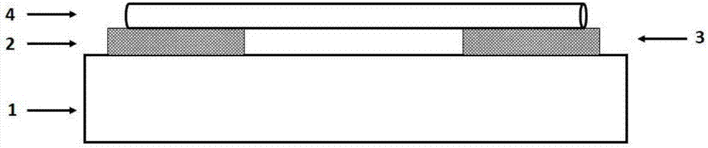
[0041] The preparation of ITO electrodes with left and right structures mainly uses photolithography and magnetron sputtering techniques.
[0042] (1) Photolithography, first use a homogenizer to evenly spin-coat the photoresist on the clean Si / SiO 2 On the substrate, the condition is to rotate at a low speed of 600 rpm for 6 seconds, and then rotate at a high speed of 2000 rpm for 15 seconds; the substrate of the spin-coated photoresist is baked at 100 ° C for 1 min; and then exposed using a mask; Develop after exposure, the ratio of the developer is tetramethylammonium hydroxide: deionized water = 1:10, the development time is 60 seconds, and then rinse in deionized water for 15 seconds; the rinsed substrate is post-baked at 100°C 1min.
[0043] (2) Sputtering, transfer the photolithographic substrate to the magnetron sputtering vacuum chamber, and place the ITO target material, the target material purity is >99.99%, and the background vacuum degree during sputtering is bet...
Embodiment 1
[0048] 1. Substrate cleaning: use the above-mentioned cleaning process for Si / SiO 2 The substrate is cleaned.
[0049] 2. Preparation of ITO electrodes: ITO electrodes were prepared by photolithography and sputtering processes as described above.
[0050] 3. Growth of perovskite micron wires: configure PbI 2 / DMF mixed solution, PbI 2 : The mass ratio of DMF is 1:9.5, stirring at 80°C to dissolve it completely, then adding a certain amount of deionized water to form a supersaturated solution, and then standing at room temperature for 10h. PB 2 Due to the precipitation of recrystallization, PbI was obtained 2 The suspension of micron wires can be stored for a long time; 2 The suspension of micron wires was spin-coated on the substrate with ITO electrodes, and annealed at 100 °C for 10 min to make PbI 2 For better crystallization, put the substrate into 3 mg / ml CsBr methanol solution for 1 hour at room temperature. Take out the substrate, clean it with isopropanol, and dr...
Embodiment 2
[0055] 1. Cleaning of the substrate: same as in Example 1.
[0056] 2. Preparation of ITO electrode: Same as Example 1.
[0057] 3. Growth of perovskite micron wires: configure PbI 2 / DMF mixed solution, PbI 2 : The mass ratio of DMF is 1:7, stirring at 70°C to dissolve it completely, then adding a certain amount of deionized water to form a supersaturated solution, and then standing at room temperature for 12 hours. PB 2 Due to the precipitation of recrystallization, PbI was obtained 2 The suspension of micron wires can be stored for a long time; 2 The suspension of micron wires was spin-coated on the substrate with ITO electrodes, and annealed at 100 °C for 10 min to make PbI 2 Better crystallization; then immerse in 3mg / ml CsBr methanol solution for 2 hours, grow to get CsPbBr 3 Perovskite Microwires. Take out the substrate, clean it with isopropanol, and dry the isopropanol with nitrogen. The obtained samples were annealed at 250 °C for 10 min.
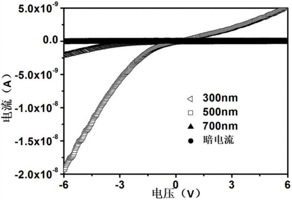
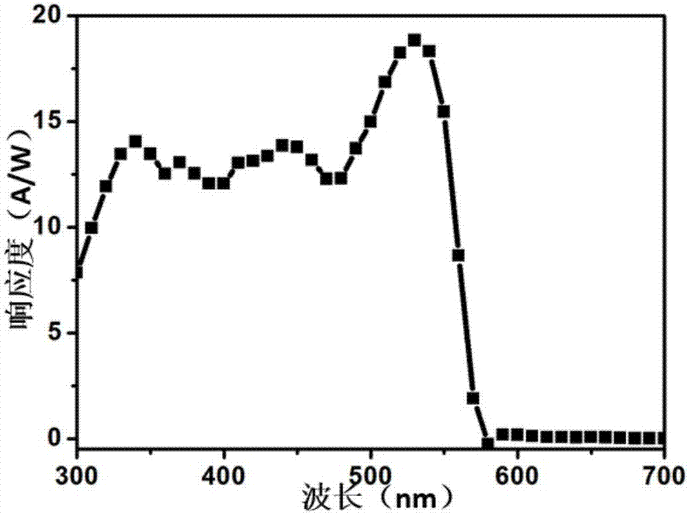
[0058] 4. Test: P...
PUM
| Property | Measurement | Unit |
|---|---|---|
| Diameter | aaaaa | aaaaa |
| Length | aaaaa | aaaaa |
Abstract
Description
Claims
Application Information
 - R&D
- Intellectual Property
- Life Sciences
- Materials
- Tech Scout
- Unparalleled Data Quality
- Higher Quality Content
- 60% Fewer Hallucinations
Browse by: Latest US Patents, China's latest patents, Technical Efficacy Thesaurus, Application Domain, Technology Topic, Popular Technical Reports.
© 2025 PatSnap. All rights reserved.Legal|Privacy policy|Modern Slavery Act Transparency Statement|Sitemap|About US| Contact US: help@patsnap.com