Negative capacitance molybdenum disulfide transistor based on ferroelectric gate dielectric and preparation method thereof

A ferroelectric gate dielectric, molybdenum sulfide technology, applied in semiconductor/solid-state device manufacturing, circuits, electrical components, etc., can solve problems such as heat generation that cannot be ignored, limit chip operating speed, and lower operating frequency upper limit, etc. Circuit integration, avoiding slow device turn-on and fast turn-on effects

Active Publication Date: 2020-03-20
贵溪穿越光电科技有限公司
View PDF8 Cites 0 Cited by
  • Summary
  • Abstract
  • Description
  • Claims
  • Application Information

AI Technical Summary

Problems solved by technology

If it is miniaturized to prepare high-density integrated circuits, especially integrated circuits with a feature size of less than 5nm, the heat generation cannot be ignored. At higher temperatures, the carriers are severely scattered by phonons, which will limit the chip The operating speed is lower, the upper limit of its operating frequency is reduced, and the performance of the chip is reduced. Compared with devices such as FinFETs of the same size, it is difficult to reflect the electrical advantages.
In addition, due to the short channel effect, traditional planar gate MoS 2 The subthreshold slope of field effect transistors will increase as the channel width becomes shorter, that is, the gate control ability deteriorates as the channel becomes shorter

Method used


Image

  • Negative capacitance molybdenum disulfide transistor based on ferroelectric gate dielectric and preparation method thereof
  • Negative capacitance molybdenum disulfide transistor based on ferroelectric gate dielectric and preparation method thereof

Examples


Embodiment Construction

[0028] The present invention will be described in detail below in conjunction with the accompanying drawings and specific embodiments.

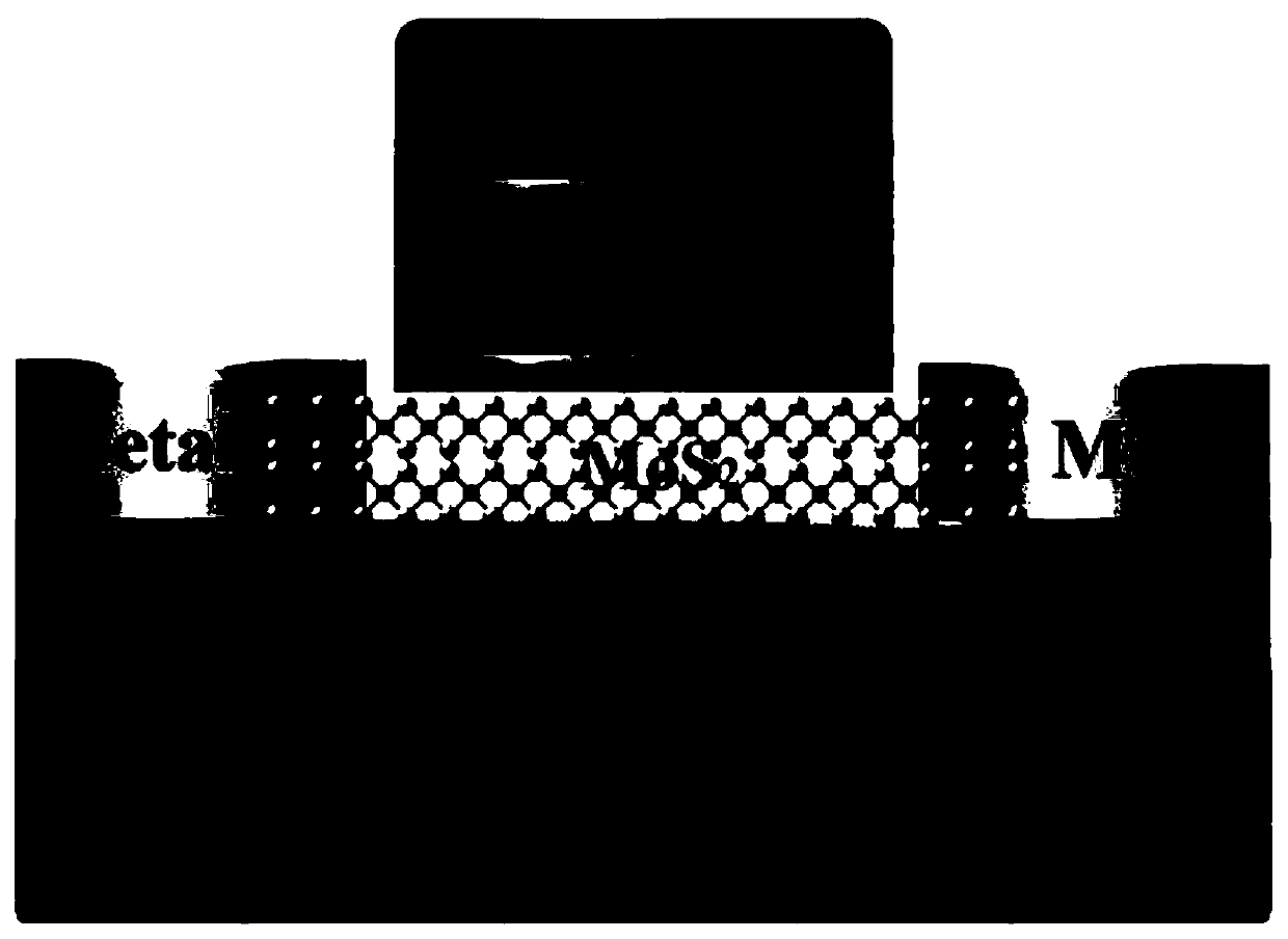
[0029] This embodiment provides a method for preparing a negative capacitance molybdenum disulfide transistor based on a ferroelectric gate dielectric. The preparation method includes, first, SiO 2 Substrates are cleaned, SiO 2 The specific cleaning process of the substrate is as follows:

[0030] 1) Ultrasonic cleaning with acetone, the ultrasonic frequency is 45-50KHz;

[0031] 2) Ethanol ultrasonic cleaning, the ultrasonic frequency is 50-55KHz;

[0032] 3) Rinse in a beaker of deionized water;

[0033] 4) Boil in concentrated sulfuric acid: hydrogen peroxide = 4:1 (volume ratio) mixture at 90°C for 15 minutes, rinse with deionized water. The concentration of sulfuric acid is 98%, and the concentration of hydrogen peroxide is 40%.

[0034] Put the cleaned material into the CVD equipment to grow molybdenum sulfide material. The CVD met...


PUM

PropertyMeasurementUnit
thicknessaaaaaaaaaa
thicknessaaaaaaaaaa
band gapaaaaaaaaaa

Abstract

The invention discloses a ferroelectric medium-based negative capacitance MoS2 transistor and a preparation method thereof. The preparation method comprises the steps of growing a MoS2 thin film on asurface of a SiO2 substrate; sequentially growing a first High-K layer, a first TiN layer, a ferroelectric thin film layer, a second TiN layer, a second High-K layer which are used as a grid dielectric layer on a surface of the MoS2 thin film; growing a third TiN layer and a Ti / Au metal layer which are used a grid electrode on the grid dielectric layer; and growing two layers of Al metal which areused a source electrode and a drain electrode on the MoS2 thin film layer. The TiN layers wrap the ferroelectric grid dielectric thin film layer, the metal TiN is used for balancing an additional electric field generated by population and turnover of the ferroelectric grid dielectric thin film again, the additional electric field is uniformly applied to the MoS2 thin film layer, the situations that the device is started slowly and a sub-threshold is relatively larger caused by different MoS2 inversion conditions of each point in a channel are prevented, and meanwhile, the situation that the point is easy to break down when point field intensity of the High-K layers is relatively large is also prevented.

Description

technical field [0001] The invention relates to the technical field of manufacturing semiconductor integrated circuits, in particular to a negative capacitance molybdenum disulfide transistor based on a ferroelectric gate dielectric and a preparation method thereof. Background technique [0002] Molybdenum disulfide (MoS 2 ) film, as a new type of two-dimensional material, is similar to graphene in structure and performance, and both have a layered structure and high carrier mobility. But compared to the zero bandgap of graphene, MoS 2 The bandgap of the film changes with the number of layers. bulk crystalline MoS 2 The bandgap of MoS is 1.20eV, and its electronic transition mode is indirect transition; when the thickness is a single layer, MoS 2 The band gap can reach 1.82eV, and its electronic transition mode is changed to direct transition. Therefore, MoS 2 The unique structure, excellent physical properties and adjustable energy bandgap of the film make it have gre...

Claims


Application Information

Patent Timeline
Patent Type & Authority Patents(China)
IPC IPC(8): H01L21/34H01L21/44H01L29/423H01L29/78
Inventor 刘新科刘强俞文杰
Owner 贵溪穿越光电科技有限公司
Why Eureka
Try Eureka