Flexible dielectric film and organic field effect transistor prepared thereby

A technology of dielectric films and transistors, applied in the field of flexible electronics, can solve problems such as low dielectric constant

Active Publication Date: 2018-01-19
FUJIAN INST OF RES ON THE STRUCTURE OF MATTER CHINESE ACAD OF SCI
View PDF4 Cites 4 Cited by
  • Summary
  • Abstract
  • Description
  • Claims
  • Application Information

AI Technical Summary

Problems solved by technology

However, the low dielectric constant (~3) of PMMA requires a high operating voltage to start OFETs, which is the main limitation faced by most polymer dielectric materials.

Method used


Image

  • Flexible dielectric film and organic field effect transistor prepared thereby
  • Flexible dielectric film and organic field effect transistor prepared thereby
  • Flexible dielectric film and organic field effect transistor prepared thereby

Examples


Embodiment approach

[0109] According to one embodiment of the present invention, the preparation method of the organic field effect transistor of the present invention is as follows:

[0110] 1. Preparation of dielectric film solution: first dissolve PAA in isopropanol, stir magnetically until dissolved at 50°C-80°C, then add PMMA and butanone to it, continue magnetic stirring for 2-6h to form a clear and transparent Mixed solution, wherein the concentration of the solution is 40-80 mg / mL, the PAA accounts for 0.1%-10% of the total mass of PMMA and PAA, and the volume ratio of isopropanol to butanone is 1-3:1;

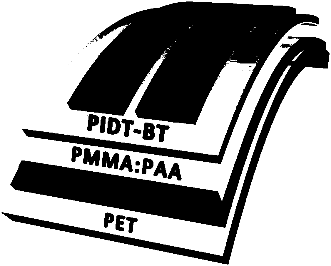
[0111] 2. Preparation of dielectric layer / gate / substrate assembly: use PET with a thickness of 50-125 μm as the substrate, and cover it with a layer of ITO. After 15 minutes of ultraviolet ozone treatment, the blend prepared in step (1) is passed through conventional The solution spin-coating technology is used to spin-coat on the substrate, and the number of spin-coating is 3 to 6 times....

Embodiment 1

[0115] 1. The bottom-gate top-contact thin film transistor structure is adopted, and the preparation process of the corresponding flexible OFET is as follows:

[0116] (1) Preparation of PMMA:PAA dielectric layer by solution spin coating method and low temperature annealing process

[0117] Step 1: Select a commercially purchased PET-ITO film (square resistance 6-8Ω / cm 2 ), wherein PET is used as the substrate, and ITO is used as the grid electrode, and it is treated with ultraviolet ozone for 15 minutes before use;

[0118] Step 2: Weigh 15mg of PAA and dissolve it in 5mL of isopropanol, stir magnetically at 70°C until dissolved, then add 585mg of PMMA and 5mL butanone to it, and continue to stir magnetically at 70°C for 4h to form clear and transparent PMMA Mixed solution with PAA;

[0119] Step 3: Spin-coat the mixed solution of PMMA and PAA prepared in step 2 on the PET-ITO that has been treated with ultraviolet ozone in advance. The number of times of spin coating is 3 ...

Embodiment 2

[0129] (1) The difference from the preparation process of the flexible OFET in Example 1 is that PAA accounts for 2.5% of the total mass of PAA and PMMA.

[0130] (2) Performance testing of flexible OFET devices:

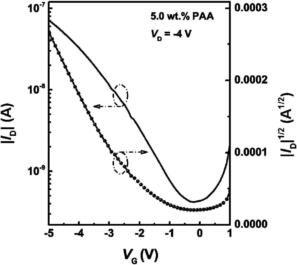
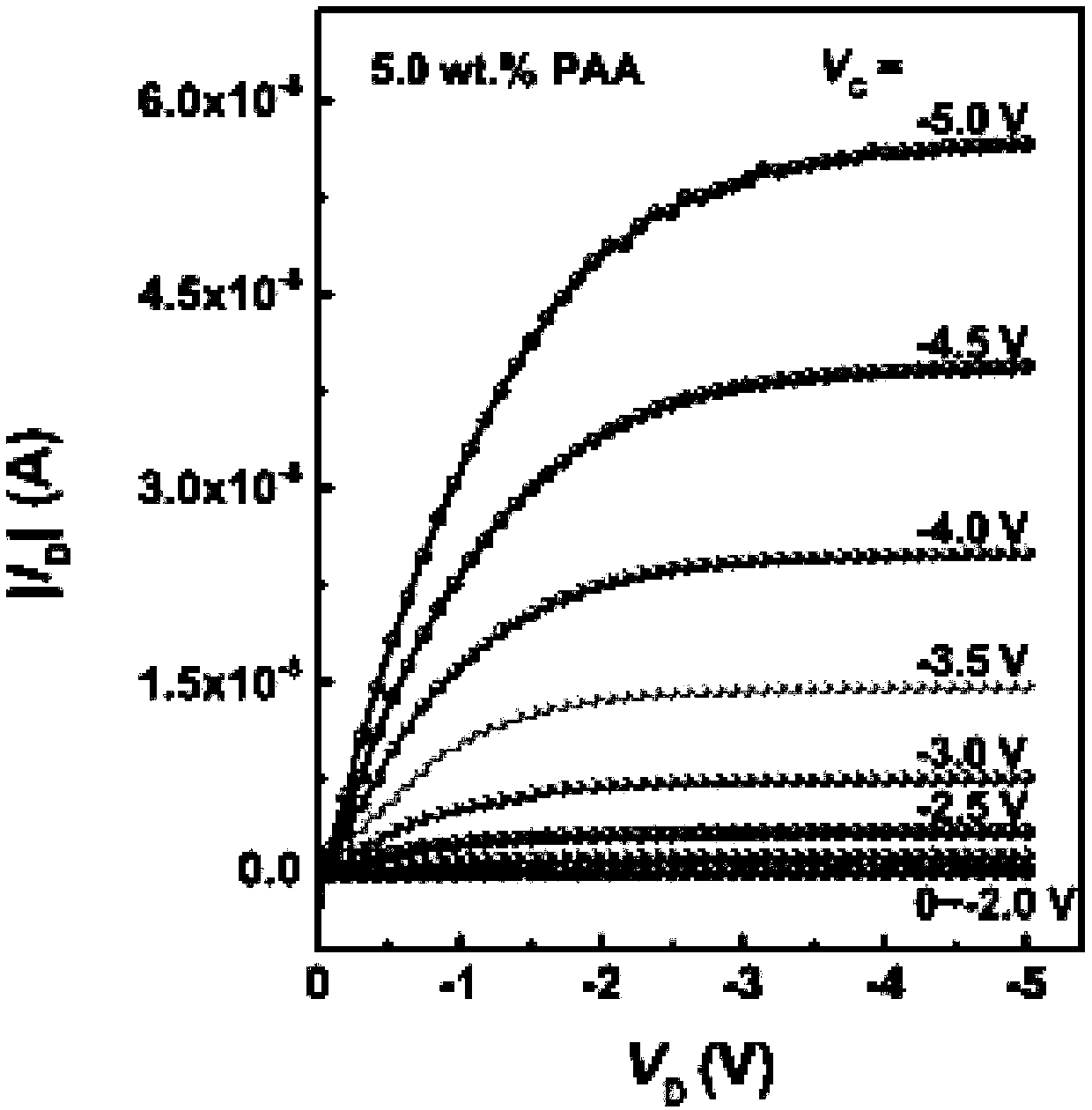
[0131] Use the Agilent 4155c Semiconductor Parameter Analyzer to test the transfer characteristic curve of the flexible OFET after bending (such as Figure 4 shown), where the source-drain voltage V D =-4V, the bending radius of the flexible OFET is r=15mm, the substrate thickness is 125μm, and the bending times are 0, 100, 200, 500, 1000 and 1500 times, respectively, and the bending times have no obvious attenuation on the electrical properties of the flexible OFET, showing good stability.


PUM

PropertyMeasurementUnit
thicknessaaaaaaaaaa
concentrationaaaaaaaaaa

Abstract

The invention provides a dielectric material, a dielectric film, a flexible organic field effect transistor (OFET) prepared by the dielectric film, a preparation method of the flexible organic field effect transistor (OFET), and the application thereof in the field of electronic equipment. The dielectric material and the dielectric film contain polymethyl methacrylate and polyacrylic acid. The thickness of the dielectric film is 1-2 microns. According to the preparation method of the flexible OFET, the dielectric film is processed on a substrate covered with a grid electrode. After that, the spin-coated treatment of an organic semiconductor layer is conducted with a solution. Finally, a source electrode and a drain electrode are evaporated. The dielectric film disclosed by the invention issmall in electricity leakage, adjustable in dielectric constant, controllable in thickness, and high in strength/flexibility. The dielectric film and the flexible OFET are good in electrical performance, and excellent in application prospect in the aspect of low-energy-consumption flexible electronic equipment. The preparation method of the dielectric film and the flexible OFET is low in cost andsimple and convenient in process.

Description

technical field [0001] The invention belongs to the technical field of flexible electronics, and in particular relates to a dielectric film, an organic field effect transistor constructed by the dielectric film, a preparation method thereof, and an application in the field of electronic equipment. Background technique [0002] In recent years, organic electronic materials and devices based on flexible substrates have attracted widespread attention worldwide, and they have good application prospects in many fields such as flexible displays, electronic skins, sensors, and wearable devices. Organic field effect transistor (OFET), as one of the important flexible electronic devices, has developed very rapidly and has become the research frontier and hotspot of organic electronics. Compared with traditional inorganic transistors, OFET processing methods are more convenient and diverse, including Langmuir-Blodgett (LB) film technology, molecular self-assembly, spin coating, scrape...

Claims


Application Information

Patent Timeline
Patent Type & Authority Applications(China)
IPC IPC(8): H01L51/05H01L51/10H01L51/40
Inventor 郑庆东尹志刚柳子杨
Owner FUJIAN INST OF RES ON THE STRUCTURE OF MATTER CHINESE ACAD OF SCI
Why Eureka
Try Eureka