Silicon carbide device and manufacturing method therefor

A manufacturing method and silicon carbide technology, which are applied in semiconductor/solid-state device manufacturing, semiconductor devices, electrical components, etc., can solve the problems of lengthening the tape-out cycle, increasing the difficulty of tape-out, and complicated preparation process, and achieving on-resistance. The effect of low, shortened tapeout cycle and simple process

Inactive Publication Date: 2018-02-02
INST OF MICROELECTRONICS CHINESE ACAD OF SCI
View PDF4 Cites 5 Cited by
  • Summary
  • Abstract
  • Description
  • Claims
  • Application Information

AI Technical Summary

Problems solved by technology

Although the use of this structure and process solves the problem of high surface roughness of the channel, the preparation process is complicated and requires - Two more epitaxial growths and

Method used


Image

  • Silicon carbide device and manufacturing method therefor
  • Silicon carbide device and manufacturing method therefor
  • Silicon carbide device and manufacturing method therefor

Examples


Embodiment Construction

[0041] In order to make the purpose, technical solutions and advantages of the embodiments of the present invention clearer, the technical solutions in the embodiments of the present invention will be clearly and completely described below in conjunction with the drawings in the embodiments of the present invention. Obviously, the described embodiments It is only some embodiments of the present invention, but not all embodiments. Based on the embodiments of the present invention, all other embodiments obtained by persons of ordinary skill in the art without making creative efforts belong to the protection scope of the present invention.

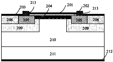
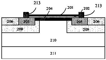
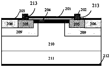
[0042] figure 1 A schematic structural diagram of an IEMOSFET device in the prior art is shown. As shown, the device includes: N + - SiC substrate 111, N + - SiC substrate 111 can be formed by heavily doping Group V impurities such as phosphorus, nitrogen, arsenic or antimony in semiconductor materials such as silicon carbide (SiC) wafers;...


PUM


Abstract

The invention provides a manufacturing method for a silicon carbide device, and the device comprises the steps: 1, providing an N+-SiC substrate, forming an N--SiC epitaxial layer on the N+-SiC substrate, and carrying out the ion implantation at two ends of the N--SiC epitaxial layer to form a P well; 2, carrying out the extension of an N-type trench layer on the surface of the device; 3, carryingout the ion implantation at two ends of the device, and forming an N+ source region and a P+ source region, which are adjacent to each other; 4, growing a gate oxidation layer on the surface of the device, growing a polycrystalline silicon layer above the gate oxidation layer, carrying out the etching, and obtaining a gate electrode; 5, depositing an interlayer medium on the surface of the gate oxidation layer, carrying out the etching of the interlayer medium and the gate oxidation layer, so as to form a contact window of the source electrode and the N+ source region and P+ source region; 6,forming the source electrode and a drain electrode on the front and back surfaces of a device. The invention also provides the silicon carbide device. The method can guarantee the depth of a conductive trench, inhibits the contact interface roughness caused by the injection technology, and simplifies the device preparation process.

Description

technical field [0001] The invention relates to the technical field of semiconductor power devices, in particular to a silicon carbide device and a manufacturing method thereof. Background technique [0002] Compared with the first-generation semiconductor represented by silicon and the second-generation semiconductor represented by gallium arsenide, the third-generation semiconductor material silicon carbide (SiC) has a larger band gap and higher critical breakdown than silicon Compared with silicon power devices of the same withstand voltage level, SiC has a higher doping concentration and a smaller epitaxial layer thickness, so the forward conduction resistance can be greatly reduced, and the power loss is greatly reduced; at the same time, carbonization Silicon has high thermal conductivity, high temperature resistance and high electron saturation rate. It is suitable for high-current and high-power applications. It can reduce the requirements for heat dissipation equipm...

Claims


Application Information

Patent Timeline
IPC IPC(8): H01L21/04H01L21/336H01L29/10H01L29/78
CPCH01L21/046H01L29/1033H01L29/66068H01L29/7827
Inventor 刘新宇郭元旭白云邓小川陈宏杨成樾汤益丹田晓丽王文刁绅徐少东
Owner INST OF MICROELECTRONICS CHINESE ACAD OF SCI
Why Eureka
Try Eureka