
Annealing method of ferric-doped indium phosphate monocrystal chips

A technology of indium phosphide and indium single crystal, which is applied in the annealing field of iron-doped indium phosphide single wafer, can solve the problems of occupying interstitial sites and reducing the activation rate of Fe, so as to increase material resistivity and improve semi-insulating properties and stability, to overcome the effect of high iron doping concentration

Inactive Publication Date: 2018-02-09
珠海鼎泰芯源晶体有限公司
View PDF1 Cites 7 Cited by
  • Summary
  • Abstract
  • Description
  • Claims
  • Application Information

AI Technical Summary

Problems solved by technology

In the iron-doped InP material prepared by vertical gradient freeze method (VGF, vertical gradient freeze method), the displacement activation of Fe is mainly through the interstitial-hopping mechanism, but Fe atoms tend to gather around dislocations and form complexes with vacancies. Occupy interstitial sites, etc., thereby reducing the activation rate of Fe

Method used


Image

  • Annealing method of ferric-doped indium phosphate monocrystal chips
  • Annealing method of ferric-doped indium phosphate monocrystal chips
  • Annealing method of ferric-doped indium phosphate monocrystal chips

Examples


Embodiment

[0050] In the present invention, the iron-doped indium phosphide single wafer is annealed, and the specific steps are as follows:

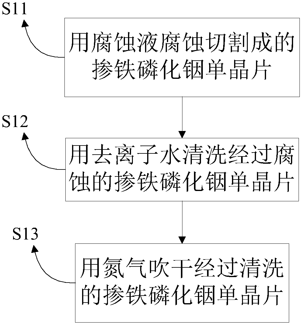
[0051] First, the iron-doped indium phosphide material prepared by the VGF method is selected, and the iron doping concentration is greater than or equal to 3×10 16 cm -3 , the dislocation density is less than or equal to 1000cm -2 , the above-mentioned iron-doped indium phosphide material was cut into pieces, chemically etched with an etching solution prepared by hydrochloric acid and nitric acid with a volume ratio of 3:1 for 2 minutes, cleaned with deionized water, and dried with nitrogen for subsequent use. use.

[0052] Secondly, choose massive red phosphorus with a purity greater than 6N, estimate the amount of red phosphorus used, put the massive red phosphorus into a quartz container, put the quartz container into a quartz tube; put the treated iron-doped indium phosphide single chip into On the quartz sample holder, put the quartz samp...


PUM


Abstract

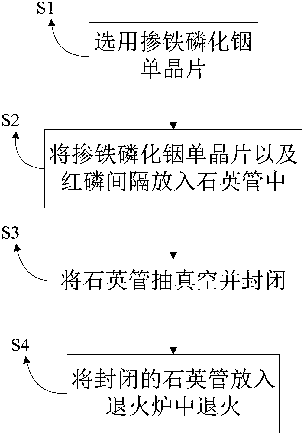
The invention discloses an annealing method of ferric-doped indium phosphate monocrystal chips. The annealing method includes the steps of S1, selecting the ferric-doped indium phosphate monocrystal chips; S2, putting the ferric-doped indium phosphate monocrystal chips and red phosphorus into a quartz tube at intervals; S3, vacuumizing and enclosing the quartz tube; S4, placing the enclosed quartztube into an annealing furnace for annealing. The ferric-doped indium phosphate monocrystal chips are subjected to annealing treatment, gathering of impurities in indium phosphate monocrystal materials is effectively avoided, defects of complexes are reduced, shortcomings of high concentration of ferric-doped indium phosphate crystal materials, poor uniformity and stability and the like are overcome, activating efficiency of ferric is effectively improved, resistivity of the materials is improved, and semi-insulation and stability of the ferric-doped phosphate monocrystal materials are improved.

Description

technical field [0001] The invention relates to the technical field of semiconductors, in particular to an annealing method for an iron-doped indium phosphide single wafer. Background technique [0002] Due to the application of semiconductor chips in various fields such as electronics, communication and energy, the development of semiconductor chips has received more and more attention. Semi-insulating indium phosphide (InP) crystal is an important compound semiconductor material. Compared with gallium arsenide (GaAs), its advantages mainly lie in high saturation electron drift speed, good thermal conductivity and strong radiation resistance. Therefore, phosphorus Indium chloride wafers are commonly used in the manufacture of high-frequency, high-speed and high-power microwave devices and circuits. As a substrate material, InP has been widely used in many fields, such as millimeter-wave heterojunction bipolar transistors (HBT), high electron mobility transistors (HEMT) and...

Claims


Application Information

Patent Timeline
IPC IPC(8): C30B33/02C30B29/40
CPCC30B29/40C30B33/02
Inventor 段满龙赵有文杨俊卢伟
Owner 珠海鼎泰芯源晶体有限公司
Learn More