Si-based vertical cavity surface emitting chip
A vertical cavity surface emission and chip technology, which is applied in phonon exciters, laser parts, semiconductor lasers, etc., can solve the problems of inability to emit light directly, and it is difficult to realize continuous operation of silicon-based VCSLE at room temperature, which is beneficial to mass production. , Compatible with the preparation process
- Summary
- Abstract
- Description
- Claims
- Application Information
AI Technical Summary
Problems solved by technology
Method used
Image

Examples
preparation example Construction
[0035] A method for preparing a Si-based vertical cavity surface emitting chip, the specific steps are as follows:
[0036](1) Clean the Si substrate 20 and treat the oxide layer on the surface of the substrate 20 with hydrofluoric acid, and epitaxially grow Ga on the treated substrate 20 by using pulsed light laser deposition or magnetron sputtering. 2 o 3 buffer layer 30;
[0037] (2) alternately growing Al-doped gallium oxide mixtures with different doping concentrations on the buffer layer 30 as the lower distributed Bragg reflector 40;
[0038] (3) Epitaxial growth of rare earth doped Ga on the lower distributed Bragg reflector 40 2 o 3 as the active layer 50;
[0039] (4) alternately growing two dielectric materials on the active layer 50 as the upper distributed Bragg reflector 60;
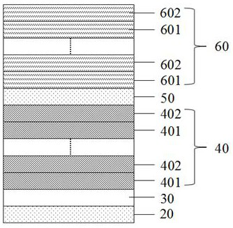
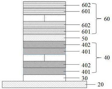
[0040] (5) An epitaxial structure composed of the buffer layer 30, the lower distributed Bragg reflector 40, the active layer 50, and the upper distributed Bragg reflector 60, such as ...
Embodiment 1
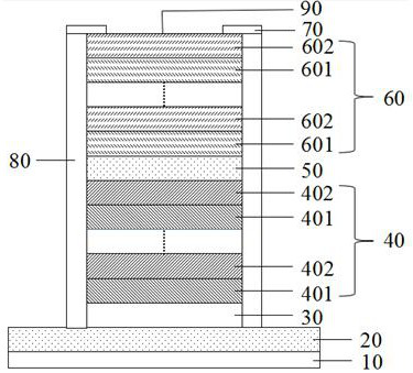
[0047] This embodiment provides a silicon-based vertical cavity surface emitting light source, such as image 3 As shown, the silicon-based VCSEL structure includes an n-type electrode 10, a substrate 20, a buffer layer 30, a lower distributed Bragg reflector 40, an active layer 50, an upper distributed Bragg reflector 60, and a p-type electrode 70. , a confinement layer 80 , and a light exit window 90 .
[0048] In this embodiment, the substrate 20 is an n-type silicon wafer, which provides support for the entire light source structure. On the substrate, the epitaxial growth buffer layer 30 is deposited by pulsed laser, and the material of the buffer layer is Ga 2 o 3 , with a thickness of 500 nm, providing a transition for growing a high-quality distributed Bragg reflector 40 . Then grow the lower distributed Bragg reflector 40 on the buffer layer, and the lower distributed Bragg reflector 40 is made of periodically grown dielectric material 401 (AlxGa1-x) 2 o 3 with 40...
Embodiment 2
[0052] This embodiment provides a silicon-based vertical cavity surface emitting light source, such as image 3 As shown, the silicon-based VCSEL structure includes an n-type electrode 10, a substrate 20, a buffer layer 30, a lower distributed Bragg reflector 40, an active layer 50, an upper distributed Bragg reflector 60, and a p-type electrode 70. , a confinement layer 80 , and a light exit window 90 .
[0053] In this embodiment, the substrate 20 is an n-type silicon wafer, which provides support for the entire light source structure. On the substrate, the epitaxial growth buffer layer 30 is deposited by pulsed laser, and the material of the buffer layer is Ga 2 o 3 , with a thickness of 500 nm, providing a transition for growing a high-quality distributed Bragg reflector 40 . Then grow the lower distributed Bragg reflector 40 on the buffer layer, and the lower distributed Bragg reflector 40 is made of periodically grown dielectric material 401 (AlxGa1-x) 2 o 3 with 40...
PUM
 Abstract
Description
Claims
Application Information
 - R&D
- Intellectual Property
- Life Sciences
- Materials
- Tech Scout
- Unparalleled Data Quality
- Higher Quality Content
- 60% Fewer Hallucinations
Browse by: Latest US Patents, China's latest patents, Technical Efficacy Thesaurus, Application Domain, Technology Topic, Popular Technical Reports.
© 2025 PatSnap. All rights reserved.Legal|Privacy policy|Modern Slavery Act Transparency Statement|Sitemap|About US| Contact US: help@patsnap.com