
Method for manufacturing MEMS atomic cavity of chip atomic clock

A chip atomic clock and the technology of its manufacturing method, which are applied in the field of atomic clocks, can solve the problems of rubidium vapor leakage and light transmittance, and achieve the effects of improving light transmittance, performance, and strength

Active Publication Date: 2018-03-27
BEIJING INST OF RADIO METROLOGY & MEASUREMENT
View PDF7 Cites 2 Cited by
  • Summary
  • Abstract
  • Description
  • Claims
  • Application Information

AI Technical Summary

Problems solved by technology

[0010] In order to solve at least one of the above technical problems, the present invention provides a method for manufacturing a MEMS atomic cavity of a chip atomic clock, which can effectively solve the problems of rubidium vapor leakage and low light transmittance generated during rubidium filling, and greatly improve MEMS Atomic cavity yield

Method used


Image

  • Method for manufacturing MEMS atomic cavity of chip atomic clock
  • Method for manufacturing MEMS atomic cavity of chip atomic clock
  • Method for manufacturing MEMS atomic cavity of chip atomic clock

Examples


Embodiment Construction

[0037] The present invention is described in detail by the following examples. It is necessary to point out that this example is only used to further illustrate the present invention, and can not be interpreted as limiting the protection scope of the present invention. Those skilled in the art can according to the above invention Some non-essential improvements and adjustments have been made to the content. In the case of no conflict, the embodiments and the features in the embodiments of the present invention can be combined with each other.

[0038] The manufacturing method of the MEMS atomic cavity of the chip atomic clock provided by the invention specifically comprises the following steps:

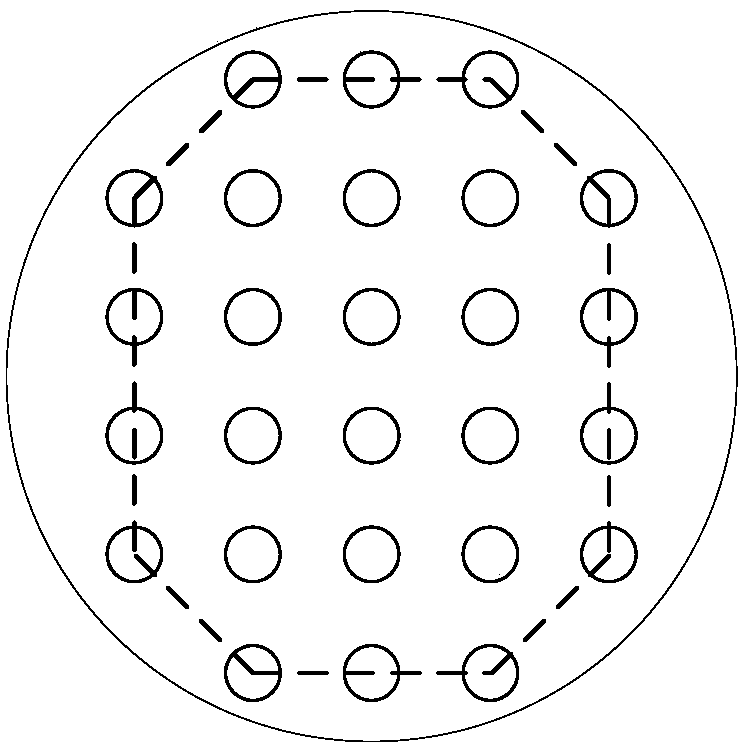
[0039] S1. Drilling and cleaning the silicon wafer: firstly, the silicon wafer is drilled, and the preferred distribution of through holes is as follows: figure 1 As shown, it is beneficial to the cutting of the MEMS atomic cavity; then the silicon wafer is cleaned to remove impuriti...


PUM


Abstract

The invention discloses a method for manufacturing an MEMS atomic cavity of a chip atomic clock. According to the method, a sealed cavity is formed by using a trough-type cover plate and a silicon wafer, so that the rubidium vapor generated by the reaction of barium azide BaN6 and rubidium chloride RbCl is separated from reaction residues, a pure rubidium atomic MEMS cavity is obtained, and the light transmittance of the MEMS atomic cavity is improved; and by accurately controlling the intensity of pressure in an anodic bonding machine, the intensity of pressure in the anodic bonding machine is slightly higher than the intensity of pressure in the MEMS cavity, the phenomenon that the leakage of the rubidium vapor does not occur in a process of second-layer silicon-glass anodic bonding canbe ensured, the rubidium filling amount in the MEMS cavity can be ensured, the contamination of rubidium atoms to a bonding interface can be prevented, the strength of anodic bonding can be increased,and the performance of the MEMS atomic cavity can also be improved. By adopting the manufacturing method disclosed by the invention, impurities in the MEMS atomic cavity can be removed, good light transmittance can be achieved, and the yield of the MEMS atomic cavity can be improved.

Description

technical field [0001] The invention relates to the technical field of atomic clocks, in particular to a method for manufacturing a MEMS atomic cavity of a chip atomic clock. Background technique [0002] Atomic clock on chip is a precision time measurement instrument. Due to its advantages of small size, light weight, low power consumption, and fast start-up speed, it can be widely used in positioning, navigation, communication, military and other fields. [0003] The miniaturization design of the physical system of the chip atomic clock adopts micro-electromechanical processing (MEMS) technology, and processes the micro-atomic gas chamber, micro-optical system, miniature magnetic field coil, magnetic shielding structure and heat preservation structure of the physical system as a whole. The miniature physical system made by MEMS process takes advantage of the heat concentration to reduce power consumption. [0004] In the miniaturization design of CPT atomic frequency stan...

Claims


Application Information

Patent Timeline
IPC IPC(8): B81C3/00B81C1/00G04F5/14
CPCB81C1/00285B81C3/001G04F5/14
Inventor 张振伟陈星杨仁福
Owner BEIJING INST OF RADIO METROLOGY & MEASUREMENT
Learn More