A quantum conductance characteristic-controllable nanocontact
A nano-dot and quantum technology, applied in the field of nanotechnology and information storage, can solve the problems of poor high-temperature retention and difficult practical application, and achieve the effects of excellent high-temperature retention, excellent fatigue resistance, high-temperature retention and stable performance.
- Summary
- Abstract
- Description
- Claims
- Application Information
AI Technical Summary
Problems solved by technology
Method used
Image

Examples
Embodiment 1
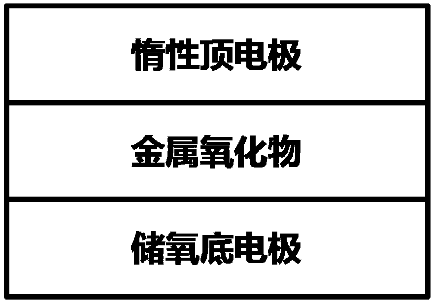
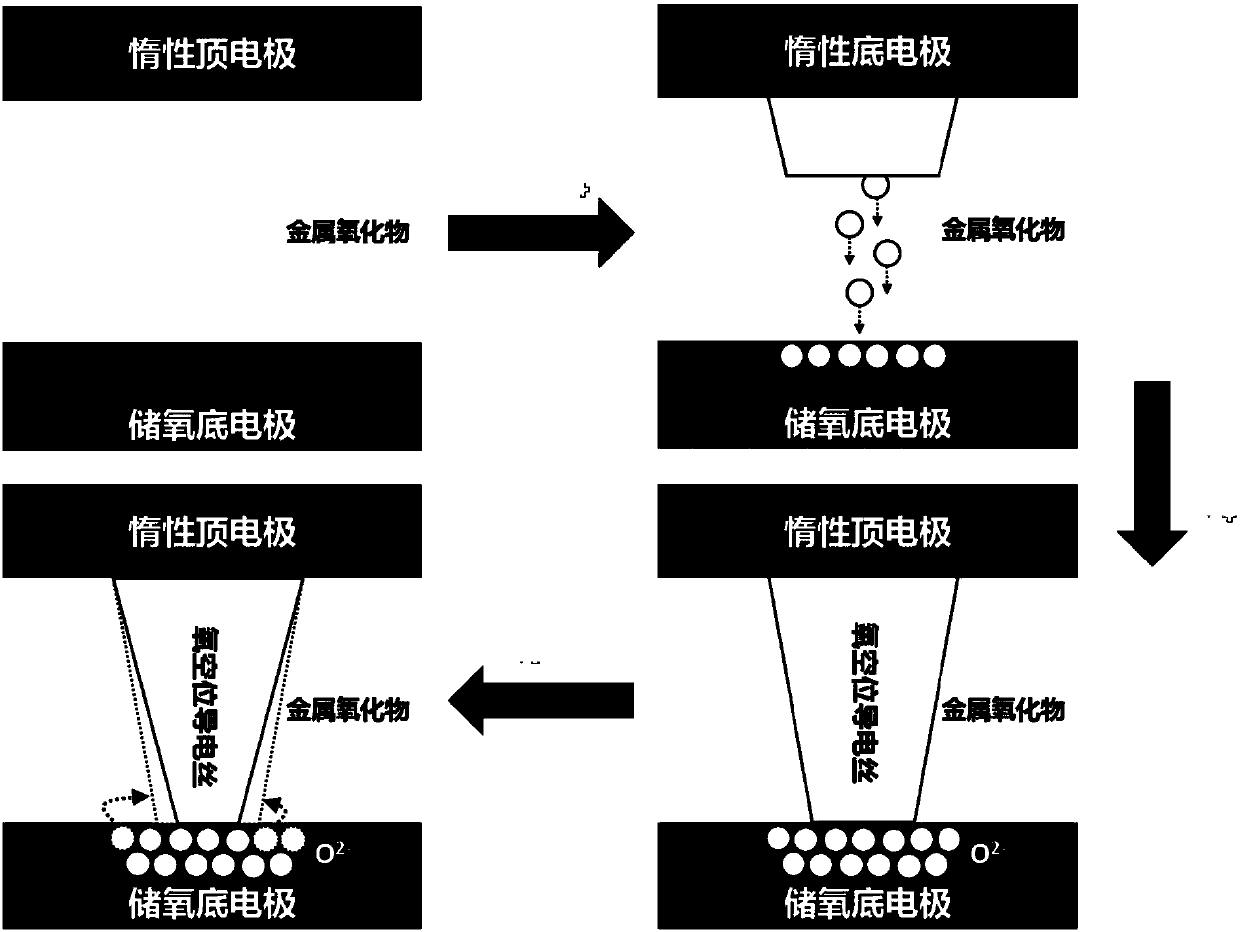
[0047] In this embodiment, the sandwich structure device such as figure 1 As shown, it includes a bottom electrode, a metal oxide and a top electrode, and the metal oxide is located between the bottom electrode and the top electrode.
[0048] In this embodiment, the bottom electrode adopts ITO with oxygen storage function; the metal oxide adopts hafnium dioxide with uniformly distributed nanometer-sized oxygen vacancy regions in the film, and the thickness is preferably 5nm-15nm; the top electrode adopts an inert Pt film with a thickness of 50nm .
[0049] In this embodiment, the sandwich structure device is prepared by coating method, including the following steps:
[0050] (1) The glass sheet coated with ITO on the surface is used as a substrate, and the substrate is ultrasonically cleaned with acetone, ethanol, and deionized water for 10 minutes, and circulated for 3 times, and then blown dry with nitrogen after taking it out;
[0051] (2) Put the substrate cleaned in ste...
Embodiment 2
[0064] In this embodiment, the sandwich structure device is completely the same as the sandwich structure device in Embodiment 1, and its preparation method is also completely the same as that in Embodiment 1.
[0065] Using Keithley 4200 semiconductor parameter measuring instrument to electrically process and characterize the sandwich structure device as follows:
[0066] (1) Forward voltage action
[0067] This process is the same as the process (1) in Example 1, so that the oxygen ions in hafnium dioxide migrate and inject into the ITO bottom electrode along the oxygen-deficient region, and form oxygen vacancy nano-conductive filaments in the oxygen-deficient region, forming a relatively large conductance value,
[0068] (2) Reverse voltage action
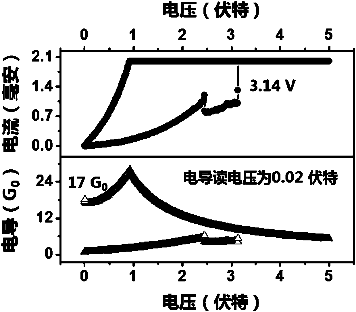
[0069] Then, the top electrode Pt is grounded, and the bottom electrode ITO is gradually applied with a negative pulse voltage, the pulse width is 20s, and the amplitude gradually increases from -0.52V to -1.92V, as Figure 7...
PUM
 Abstract
Description
Claims
Application Information
 - R&D
- Intellectual Property
- Life Sciences
- Materials
- Tech Scout
- Unparalleled Data Quality
- Higher Quality Content
- 60% Fewer Hallucinations
Browse by: Latest US Patents, China's latest patents, Technical Efficacy Thesaurus, Application Domain, Technology Topic, Popular Technical Reports.
© 2025 PatSnap. All rights reserved.Legal|Privacy policy|Modern Slavery Act Transparency Statement|Sitemap|About US| Contact US: help@patsnap.com