Nitrogen-containing polar blue-violet LED chip with polarization-induced p-type doping layer and preparation method
An LED chip, polarization-induced technology, applied in semiconductor devices, electrical components, circuits, etc., can solve problems such as low activation efficiency of Mg, improve internal quantum efficiency, improve concentration, thermal stability, and good temperature stability Effect
- Summary
- Abstract
- Description
- Claims
- Application Information
AI Technical Summary
Problems solved by technology
Method used
Image
Examples
Embodiment 1
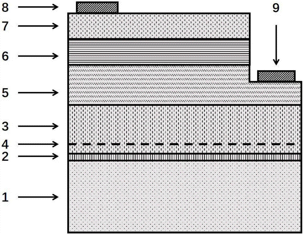
[0023]1. Adopt the MOCVD method, at first the (0001) plane sapphire substrate (circle, diameter 2 inches, bevelled direction is partial axis direction, the bevel angle is 0.8°) for high-temperature nitriding, and then one-time epitaxy on the substrate to prepare the N-polar blue-violet LED structure, such as figure 1 shown. The specific structure is as follows: a low-temperature GaN buffer layer 2 (thickness 10nm), a nitrogen-polar GaN template layer 3 (thickness 300nm), an in-situ SiN x Mask layer 4 (growth time 120s), nitrogen polarity GaN template layer 3 (thickness 1.7 μm), n-GaN electron injection layer 5 (Si doping concentration 2×10 18 / cm 3 , thickness 0.5μm), InGaN multi-quantum well active layer 6 (the number of quantum well pairs is 2 pairs, that is, well-barrier-well-barrier layer structure, the barrier layer is GaN, the thickness is 13nm, and the well layer is In 0.1 Ga 0.9 N, thickness 2nm), polarization-induced p-type doped hole injection layer 7 (Al compos...
PUM
 Abstract
Description
Claims
Application Information


