Extended wavelength table-top type avalanche photodiode and preparation method thereof
An avalanche photoelectric, mesa-type technology, applied in circuits, electrical components, semiconductor devices, etc., to achieve the effect of reducing dark current
- Summary
- Abstract
- Description
- Claims
- Application Information
AI Technical Summary
Problems solved by technology
Method used
Image
Examples
specific Embodiment
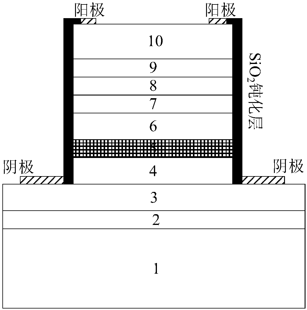
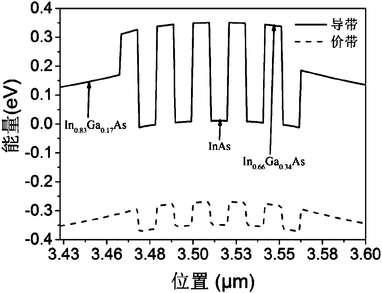
[0064] (1) Material structure growth. Using GSMBE, a 1 μm thick N-InP buffer layer was epitaxially grown sequentially on an N-type heavily doped InP substrate with a doping concentration of 2×10 18 cm -3 ; 2μm thick N-In (1-x) al x As linear gradient buffer layer, the doping concentration is 6.6×10 16 cm -3 ; 0.7μm thick N-In 0.83 Ga 0.17 As absorbing layer, the doping concentration is 1×10 16 cm -3 ; 100nm thick N-In 0.66 Ga 0.34 As / InAs superlattice, the doping concentration is 1×10 16 cm -3 ; 0.7 μm thick N - -In 0.83 Ga 0.17 As absorbing layer, the doping concentration is 1×10 16 cm -3 ; 0.25 μm thick N-InP charge layer with a doping concentration of 1×10 17 cm -3 ; 0.5 μm thick intrinsic doped InP multiplication layer; 2.0 μm thick P-type heavily doped InP contact layer with a doping concentration of 1×10 19 cm -3 .
[0065] (2) deposited silicon dioxide (SiO 2 ) mask. A layer of 700nm thick SiO was deposited on the device surface by plasma enhanced...
PUM
| Property | Measurement | Unit |
|---|---|---|
| Thickness | aaaaa | aaaaa |
| Thickness | aaaaa | aaaaa |
| Doping concentration | aaaaa | aaaaa |
Abstract
Description
Claims
Application Information
 - R&D Engineer
- R&D Manager
- IP Professional
- Industry Leading Data Capabilities
- Powerful AI technology
- Patent DNA Extraction
Browse by: Latest US Patents, China's latest patents, Technical Efficacy Thesaurus, Application Domain, Technology Topic, Popular Technical Reports.
© 2024 PatSnap. All rights reserved.Legal|Privacy policy|Modern Slavery Act Transparency Statement|Sitemap|About US| Contact US: help@patsnap.com


