Photoelectric flexible interconnection substrate and manufacturing technology thereof

A substrate and optoelectronic technology, applied in printed circuit manufacturing, multi-layer circuit manufacturing, circuit lamination, etc., to achieve the effects of reducing interconnection distance, improving high-density assembly, and saving production costs

Inactive Publication Date: 2018-05-11
NO 30 INST OF CHINA ELECTRONIC TECH GRP CORP
View PDF4 Cites 7 Cited by
  • Summary
  • Abstract
  • Description
  • Claims
  • Application Information

AI Technical Summary

Problems solved by technology

[0004] In order to overcome the above-mentioned shortcomings of the prior art, the present invention provides a photoelectric flexible interconnection substrate and its manufacturing process, which is compatible with the traditional printed circuit board manufacturing process technology, so as to avoid the loss of optical fibers in the high-temperature and high-pressure lamination process environment. Problems such as severe deformation and high temperature degradation affect optical signal transmission, realizing high-speed and high-density interconnection between boards

Method used


Image

  • Photoelectric flexible interconnection substrate and manufacturing technology thereof
  • Photoelectric flexible interconnection substrate and manufacturing technology thereof
  • Photoelectric flexible interconnection substrate and manufacturing technology thereof

Examples


Embodiment Construction

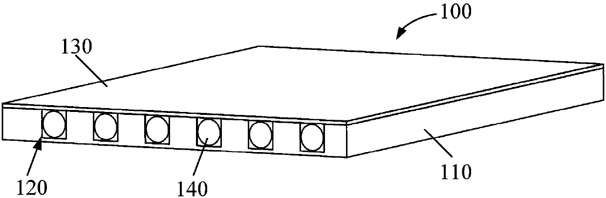
[0015] figure 1 The flexible optical circuit board 100 , which is the optoelectronic flexible interconnection substrate of the present invention, includes a flexible interconnection substrate 110 , a semi-cured gel layer 130 , and a high-temperature-resistant bare optical fiber 140 . Several high-precision positioning grooves 120 are made on the flexible interconnection substrate 110 by laser etching technology, and the high-temperature-resistant bare optical fiber 140 is embedded in the positioning grooves 120, and then a semi-cured colloid layer 130 is formed on the flexible interconnection substrate 110. The colloid layer 130 includes materials such as acrylic or epoxy resin, and the thickness can be 12.5 microns, 25 microns, 50 microns, etc.

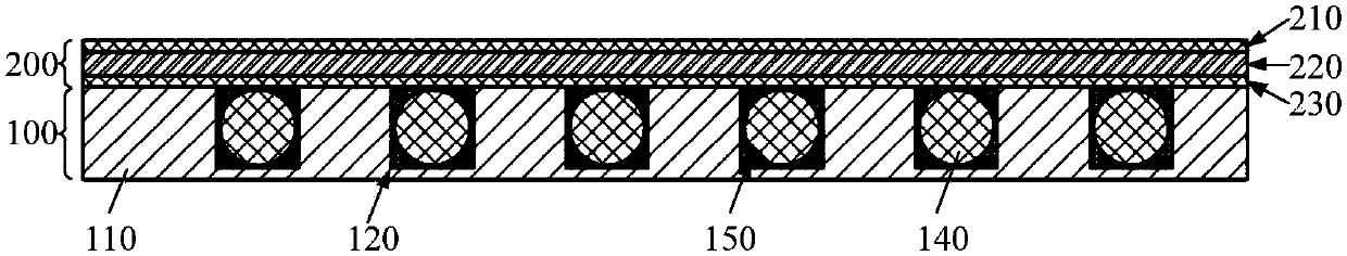
[0016] figure 2 It is a schematic diagram of the optoelectronic flexible interconnection substrate of the present invention, and the optoelectronic flexible substrate of the present invention is composed of a flexible optical circu...


PUM


Abstract

The invention discloses a photoelectric flexible interconnection substrate and a manufacturing technology thereof. The photoelectric flexible interconnection substrate comprises a flexible circuit board and a flexible optical circuit board, wherein a bonding layer is arranged between the flexible circuit board and the flexible optical circuit board; the flexible optical circuit board comprises a flexible interconnection substrate and a semi-cured colloid layer arranged on the upper surface of the flexible interconnection substrate; a positioning groove is formed in the flexible interconnectionsubstrate; a high temperature-resistant bare optical fiber is buried into the positioning groove; and the flexible circuit board comprises a copper circuit layer and a protection layer arranged on the copper circuit layer. The photoelectric flexible interconnection substrate is compatible with the manufacturing technology of a traditional printed circuit board, so that the optical fiber is takenas one layer in the flexible circuit board, an optical signal can be transmitted and lamination process and equipment do not need to be developed for the photoelectric flexible interconnection substrate; deformation, damage and high-temperature degradation of the optical fiber due to high temperature and high pressure in the lamination process can be avoided; and the bending radius of the interconnection substrate can be reduced, the interconnection distance between the boards is reduced and high-density assembly of an electronic communication system is improved.

Description

technical field [0001] The invention relates to a photoelectric flexible interconnect substrate and a manufacturing process thereof. Background technique [0002] With the rapid development of high-speed communication technology, the amount of information is increasing exponentially, which puts forward higher requirements for bandwidth, high speed, large capacity, low bit error rate and anti-electromagnetic interference ability of information transmission and exchange systems. Board-level circuits play a dominant role in electronic communication systems, and traditional electrical interconnection methods, due to their inherent physical characteristics, will lead to serious signal delays and crosstalk, limited bandwidth, and sharp increases in power consumption at high frequencies. Integrating technical difficulty and performance cost, the existing electrical interconnection mode has become a bottleneck restricting the rapid development of high-speed communication systems. T...

Claims


Application Information

Patent Timeline
Patent Type & Authority Applications(China)
IPC IPC(8): H05K1/02H05K1/14H05K3/28H05K3/36H05K3/46
CPCH05K1/0274H05K1/147H05K3/284H05K3/361H05K3/4611H05K2201/0206H05K2203/06
Inventor 毛久兵杨伟李建平冯晓娟杨平吴圣陶刘恒刘平王锐锋杨剑
Owner NO 30 INST OF CHINA ELECTRONIC TECH GRP CORP
Why Eureka
Try Eureka