Double-layer photoresist-based photonic crystal scintillator preparation method
A double-layer photoresist and photonic crystal technology, applied in the field of nuclear radiation detection, can solve the problems of optimization effect, impossibility, shallow etching depth, etc.
- Summary
- Abstract
- Description
- Claims
- Application Information
AI Technical Summary
Problems solved by technology
Method used
Image


Examples
Embodiment 1
[0028] A preparation method of photonic crystal scintillator based on double-layer photoresist, and its process flow is as follows figure 1 As shown, the following steps are taken:
[0029] Select quartz substrate 1, such as figure 1 As shown in (a), after it is cleaned, a 50nm thick PMMA is spin-coated on the upper surface of the substrate 1 as the positive glue layer 2 (manufacturer: MicroChem Corp. glue model: 950PMMA A2), Then spin-coated a layer of 100nm thick HSQ as the negative layer 3, (manufacturer: Dow Corning glue model: XR-1541-004), such as figure 1 As shown in (b).
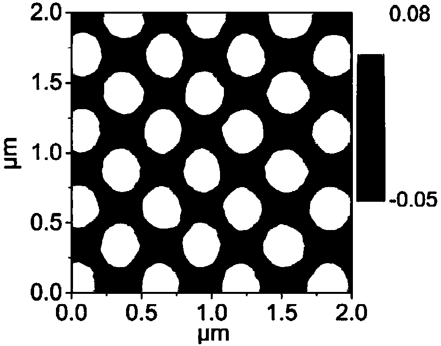
[0030] A mask consisting of four gratings is used for X-ray interference lithography. The lithography experiment was completed on the X-ray interference lithography line station of the Shanghai Synchrotron Radiation Facility (BL08U1B). After photolithography, a two-dimensional square periodic array is formed, the lattice constant is 400nm, the soft X-ray energy is 92.5eV, the single exposure time is abou...
Embodiment 2
[0036] A preparation method of photonic crystal scintillator based on double-layer photoresist adopts the following steps:
[0037] (1) First spin-coated PMMA photoresist with a thickness of 50nm as a positive glue on the cleaned quartz substrate surface, and then spin-coated a layer of HSQ photoresist with a thickness of 100nm as a negative glue;
[0038] (2) Using synchrotron radiation soft X-ray interference lithography, four beam splitting gratings are used to superimpose the first-order diffraction interference, and the photoresist on the sample surface is exposed for 15 seconds in the interference superimposed light field area. If the single exposure area Smaller, you can use multiple exposure splicing technology to obtain a larger area sample preparation. After exposure, the structure pattern of HSQ glue is obtained, and after development, a periodic structure of photoresist columnar structure composed of HSQ glue after curing is obtained;
[0039] (3) The obtained structure i...
Embodiment 3
[0043] A preparation method of photonic crystal scintillator based on double-layer photoresist adopts the following steps:
[0044] (1) First spin-coated PMMA photoresist with a thickness of 70nm on the surface of the cleaned quartz substrate as a positive resin, and then spin-coated a layer of HSQ photoresist with a thickness of 110nm as a negative resin;
[0045] (2) Using synchrotron radiation soft X-ray interference lithography, four beam splitting gratings are used to superimpose their first-order diffraction interference, and the photoresist on the sample surface is exposed for 20 seconds in the interference superimposed light field area. If the single exposure area Smaller, you can use multiple exposure splicing technology to obtain a larger area sample preparation. After exposure, the structure pattern of HSQ glue is obtained, and after development, a periodic structure of photoresist columnar structure composed of HSQ glue after curing is obtained;
[0046] (3) The obtained ...
PUM
| Property | Measurement | Unit |
|---|---|---|
| thickness | aaaaa | aaaaa |
| thickness | aaaaa | aaaaa |
| thickness | aaaaa | aaaaa |
Abstract
Description
Claims
Application Information
 - R&D
- Intellectual Property
- Life Sciences
- Materials
- Tech Scout
- Unparalleled Data Quality
- Higher Quality Content
- 60% Fewer Hallucinations
Browse by: Latest US Patents, China's latest patents, Technical Efficacy Thesaurus, Application Domain, Technology Topic, Popular Technical Reports.
© 2025 PatSnap. All rights reserved.Legal|Privacy policy|Modern Slavery Act Transparency Statement|Sitemap|About US| Contact US: help@patsnap.com