A capacitive mems gas sensor
A gas sensor, capacitive technology, applied in the direction of material capacitance, etc., can solve the problems of high environmental requirements, sensor poisoning, and many limiting factors, and achieve the effect of strong anti-electromagnetic interference ability, fast dynamic response speed, and good accuracy and stability.
- Summary
- Abstract
- Description
- Claims
- Application Information
AI Technical Summary
Problems solved by technology
Method used
Image
Examples
Embodiment 1
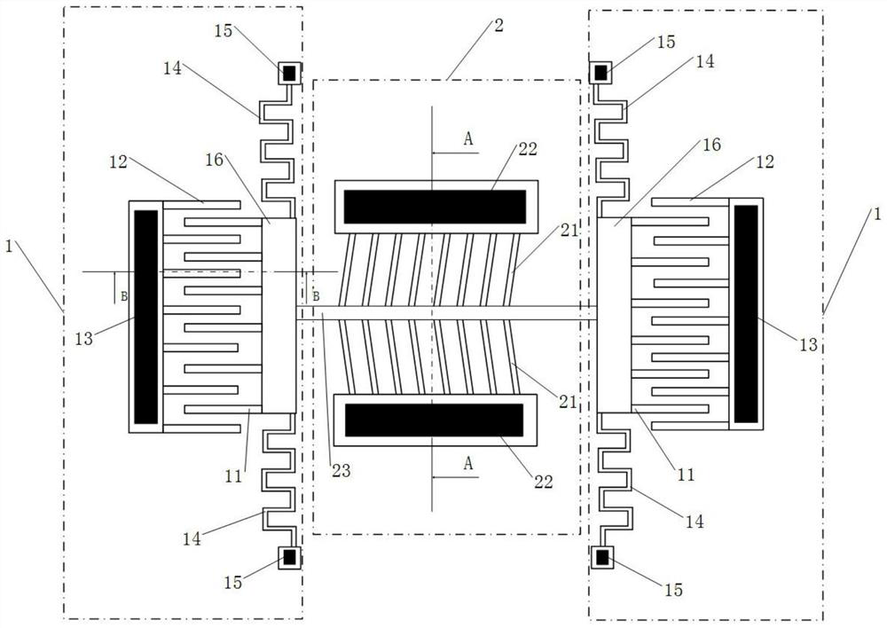
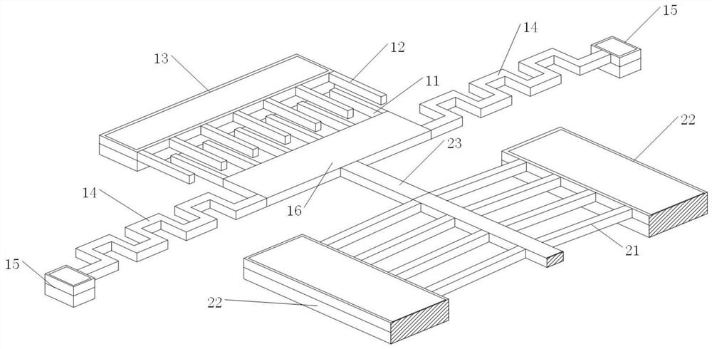
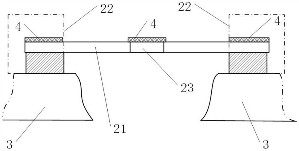
[0018] The principle of the present invention is that the resistance of the semiconductor material changes with the change of the methane concentration in the ambient gas under a certain temperature condition, and the silicon beam is made of doped single crystal silicon, and a plurality of silicon beams are connected in parallel, and the micro shuttle and the silicon beam are connected in parallel. After the anchor area forms a thermal actuator, a current excitation is applied between the silicon beams. The degree of mechanical deformation after heating is related to the change of its own resistance. The deformation of the thermal actuator drives the capacitance value of the comb capacitor to change, so the capacitance value is used Changes can indicate the concentration of methane.
[0019] According to the experimental measurement, at a certain temperature, when the silicon beam made of doped single crystal silicon is placed in the air, when a certain value of current is appl...
Embodiment 2
[0025] In this example, a specific preparation method of the sensor in Example 1 is described. Specifically, such as Figure 5 shown, including the following steps:
[0026] In the first step, doping is carried out on the SOI silicon wafer including the top layer of silicon, the first silicon dioxide buried layer, and the silicon substrate (3) by diffusion or ion implantation, so that the top layer of silicon can form N-type silicon or P-type silicon ;
[0027] In the second step, a second silicon dioxide layer is prepared on the top layer of silicon;
[0028] The third step is to etch the micro-shuttle region of the second silicon dioxide layer to form the window required for doping;
[0029] The fourth step is to use diffusion or ion implantation to form P-type silicon or N-type silicon in the micro-shuttle (23) region, and the conductivity type of the micro-shuttle region is opposite to that of the top layer of silicon;
[0030] The fifth step is to use hydrofluoric aci...
Embodiment 3
[0039] In the present embodiment, the measurement method of the MEMS capacitive gas sensor of the present invention is specifically introduced, specifically, the following steps may be included:
[0040] (1) Measure the capacitance difference △C of the two comb-tooth capacitors when the MEMS gas sensor is static 0
[0041] (2) At normal temperature and in air, calibrate the corresponding table between the concentration of the gas to be tested and the capacitance change value;
[0042] (3) Apply a first current to the anchor zone III (22), and test the capacitance difference ΔC between the two comb teeth when the thermal actuator is not in action, and the ΔC is a compensation value;
[0043] (4) Apply the measurement current to the anchor area III (22), and test the capacitance difference ΔC of the two combs 1 ;
[0044] (5) The capacitance difference △C 1 The compensation value ΔC is removed, and the corresponding table is compared to obtain the measured gas concentration....
PUM
 Abstract
Description
Claims
Application Information


