Laminated thin-film solar cell based on Sb2S3 top battery and preparation method of laminated thin-film solar cell
A solar cell and top cell technology, applied in circuits, electrical components, photovoltaic power generation, etc., can solve the problems of complex process, inability to fully utilize the solar spectrum, and high cost, achieve high spectral absorption coefficient, improve photoelectric conversion efficiency, and improve efficiency. Effect
- Summary
- Abstract
- Description
- Claims
- Application Information
AI Technical Summary
Problems solved by technology
Method used
Image
Examples
Embodiment 1
[0037] Material preparation 1. Synthesis of PbS quantum dots with different band gaps:
[0038] 1) Put 2.25g of PbO, 7.5mL of oleic acid, and 20mL of 1-octadecene (ODE) into a 50mL round-bottomed three-necked flask, seal it, heat and stir at 100°C and vacuumize for 16 hours until the PbO in the reaction flask Complete reaction forms a uniform and transparent solution to obtain a lead precursor.
[0039] 2) Take 700 μL of hexamethyldisilathane (TMS) and dissolve it in 10 mL of ODE pumped with water and oxygen as a sulfur source for use. Introduce an appropriate amount of nitrogen into the obtained lead precursor, adjust the temperature to between 90°C and 150°C, quickly inject sulfur source into the lead precursor solution, turn off the heating device, and naturally cool to room temperature to obtain a mixed solution .
[0040] 3) Take out the mixed solution and add an appropriate amount of acetone, put it into a centrifuge and centrifuge to precipitate, then remove the super...
Embodiment 2
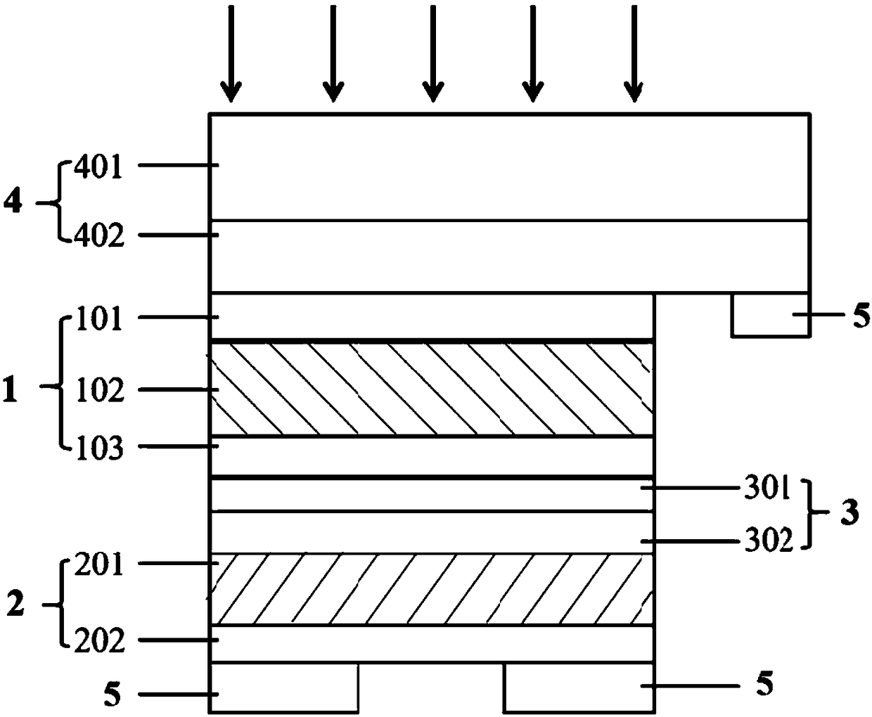
[0060] (1) Use detergent, deionized water, isopropanol, and absolute ethanol to ultrasonically clean the ITO transparent conductive glass with a resistance of 5Ω and a thickness of 100nm for 30 minutes each, and then dry it with nitrogen.
[0061] (2) A CdS buffer layer with a thickness of 40nm was deposited on the surface of ITO by chemical water bath deposition method, the temperature of the water bath was 78°C, and the deposition time was 16.5 minutes.
[0062] (3) Evaporate Sb on the CdS buffer layer by using the near-space rapid thermal evaporation method 2 S 3 Thin film absorber, 0.4gSb 2 S 3 Sprinkle the powder evenly on the square glass sheet with a side length of 2.5 cm, and the sample of the same size is inverted at a distance Sb 2 S 3 1 cm above the uniform powder, cover with a graphite block, use infrared heating, use a crystallization temperature of 300 ° C and an evaporation temperature of 550 ° C, and the evaporation time is 20 seconds, and deposit Sb with a...
Embodiment 3
[0070] (1) Use detergent, deionized water, isopropanol, and absolute ethanol to ultrasonically clean the ITO transparent conductive glass with a resistance of 60Ω and a thickness of 250nm for 30 minutes each, and then dry it with nitrogen.
[0071] (2) A CdS buffer layer with a thickness of 100 nm was deposited on the surface of ITO by chemical water bath deposition method, the temperature of the water bath was 78° C., and the deposition time was 16.5 minutes.
[0072] (3) Evaporate Sb on the CdS buffer layer by using the near-space rapid thermal evaporation method 2 S 3 Thin film absorber, 0.4gSb 2 S 3 Sprinkle the powder evenly on the square glass sheet with a side length of 2.5 cm, and the sample of the same size is inverted at a distance Sb 2 S 3 1 cm above the uniform powder, cover with a graphite block, use infrared heating, use 300 ° C crystallization temperature and 550 ° C evaporation temperature, evaporation time 20 seconds, deposit Sb with a thickness of 350 nm ...
PUM
 Abstract
Description
Claims
Application Information


