Perovskite light emitting diode with compounds containing CH2CH2O and method for preparing perovskite light emitting diode

An ethoxylate, light-emitting diode technology, applied in semiconductor/solid-state device manufacturing, electrical components, electrical solid-state devices, etc., can solve the problems of large leakage current, poor quality of perovskite films, low efficiency of light-emitting diodes, etc. The effect of improving device efficiency

Active Publication Date: 2018-07-13
SUZHOU UNIV
View PDF3 Cites 12 Cited by
  • Summary
  • Abstract
  • Description
  • Claims
  • Application Information

AI Technical Summary

Problems solved by technology

Due to the low solubility of cesium halide in commonly used perovskite precursor solvents (such as dimethyl sulfoxide, dimethylformamide), halomethylamine solvents are easy to volatilize in perovskite films, so the quality of perovskite films (continuity, uniformity...

Method used


Image

  • Perovskite light emitting diode with compounds containing CH2CH2O and method for preparing perovskite light emitting diode
  • Perovskite light emitting diode with compounds containing CH2CH2O and method for preparing perovskite light emitting diode
  • Perovskite light emitting diode with compounds containing CH2CH2O and method for preparing perovskite light emitting diode

Examples


Embodiment 1

[0059] This embodiment provides a method for preparing a perovskite film as an active light-emitting layer in a perovskite light-emitting diode, comprising the following steps:

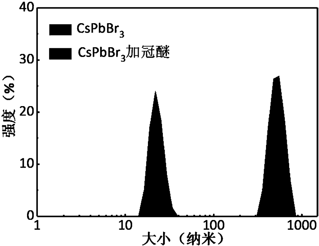
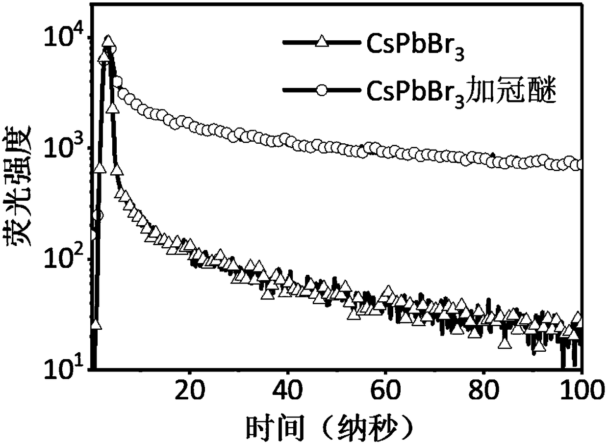
[0060] Use dimethyl sulfoxide (DMSO) as solvent to configure CsPbBr 3 Perovskite precursor solution. Wherein the molar ratio of cesium bromide and lead bromide in the precursor solution is 1:1. In the solution, the concentrations of cesium bromide and lead bromide are both 0.2mol / L. The precursor solution contained 6 mg / mL of 18-crown-6. The precursor solution prepared above was heated and stirred at 80° C. for 2 hours, and then used. Put the configured precursor solution into a cuvette, and conduct a dynamic laser light scattering experiment to obtain particle size distribution data. The prepared precursor solution was spin-coated on a quartz glass sheet at a rotation speed of 3000 rpm, the spin-coating time was 60 seconds, and annealed at 100° C. for 1 minute to obtain a perovskite film.

[006...

Embodiment 2

[0066] see Figure 4 , the present embodiment provides a three-dimensional perovskite light-emitting diode, including an anode substrate 1, a hole transport layer 2, an active light-emitting layer 3, an electron transport layer 4 (40nm), and a cathode modification layer arranged in sequence from bottom to top. 5 (1 nm) and cathode 6 (80-100 nm). Its preparation method comprises the following steps:

[0067] Use dimethyl sulfoxide (DMSO) as solvent to configure CsPbBr 3 Perovskite precursor solution. Wherein the molar ratio of cesium bromide and lead bromide in the precursor solution is 1:1. In the solution, the concentrations of cesium bromide and lead bromide are both 0.2mol / L. The precursor solution contained 6 mg / mL of 18-crown-6. The precursor solution prepared above was heated and stirred at 80° C. for 2 hours, and then used.

[0068] The ITO transparent anode substrate 1 was ultrasonically cleaned with acetone, ethanol, and deionized water for 20 minutes in sequenc...

Embodiment 3

[0078] This embodiment provides a two-dimensional perovskite light-emitting diode, including an anode substrate 1, a hole transport layer 2 (50nm), an active light-emitting layer 3 (40nm), and an electron transport layer 4 ( 30nm), cathode modification layer 5 (1nm) and cathode 6 (80-100nm). Its preparation method comprises the following steps:

[0079] Use dimethyl sulfoxide (DMSO) as solvent to configure CsPbBr 3 Perovskite precursor solution. Wherein the molar ratio of cesium bromide and lead bromide in the precursor solution is 1:1. In the solution, the concentrations of cesium bromide and lead bromide are both 0.2mol / L. The concentration of phenylethylamine is 0.08mol / L. The precursor solution contained 6 mg / mL of 18-crown-6. The precursor solution prepared above was heated and stirred at 80° C. for 2 hours, and then used.

[0080] The ITO transparent anode substrate 1 was ultrasonically cleaned with acetone, ethanol, and deionized water for 20 minutes in sequence, ...


PUM

PropertyMeasurementUnit
Thicknessaaaaaaaaaa
Thicknessaaaaaaaaaa
Thicknessaaaaaaaaaa

Abstract

The invention relates to a perovskite light emitting diode with compounds containing CH2CH2O. The perovskite light emitting diode comprises a substrate, a hole transport layer, an active light emitting layer, an electron transport layer, electrode modification layers and electrodes. The thickness of the active light emitting layer is 5-100 nanometers, the active light emitting layer comprises perovskite and the compounds containing the CH2CH2O, and the compounds containing the CH2CH2O are doped in the perovskite; the molecular formula of the perovskite is MAPbX3, FAPbX3 or CsPbX3, wherein X represents one or two of Cl, Br and I; the compounds containing the CH2CH2O are 12-crown ether-4, 15-crown ether-5, benzo-15-crown ether-5, 18-crown ether-6 and the like. The invention further providesa method for preparing the perovskite light emitting diode. The method includes: forming the hole transport layer or the electron transport layer on the substrate; modifying a perovskite precursor solution with the compounds containing the CH2CH2O on the hole transport layer or the electron transport layer to form the active light emitting layer; sequentially forming the electron transport layer,the negative electrode modification layer and the negative electrode at the top of the active light emitting layer or sequentially forming the hole transport layer, the positive electrode modificationlayer and the positive electrode at the top of the active light emitting layer; carrying out encapsulation.

Description

technical field [0001] The invention relates to the technical field of photoelectric devices, in particular to a perovskite light-emitting diode containing ethylene oxide compound and a preparation method thereof. Background technique [0002] Perovskite light emitting diode (PeLED) is a new functional device after Organic light emitting diode (OLED) and Quantumdot light emitting diode (QLED). Compared with the latter, the former mainly uses perovskite (ABX 3 ) as a luminescent material, where A is a monovalent cation (MA + 、FA + etc.), B is a divalent cation (Pb + etc.), X is a negative monovalent halide anion (Cl - 、Br - , I - ). Other than that, the device design and working principle are similar to the latter. Compared with organic light-emitting materials and quantum dots, perovskite materials have more outstanding advantages: higher color purity (the width at half-height of the luminescence peak is about 20nm), more convenient solution processing, and a wider e...

Claims


Application Information

Patent Timeline
IPC IPC(8): H01L51/54H01L51/56
CPCH10K85/30H10K71/00
Inventor 孙宝全宋涛班沐阳
Owner SUZHOU UNIV
Why Eureka
Try Eureka