Method for preparing enhanced GaN field effect device

A gallium nitride field and enhanced technology, which is applied in semiconductor/solid-state device manufacturing, semiconductor devices, electrical components, etc., can solve problems such as lattice damage, damage barrier layer surface current, and difficult precise control, so as to improve device reliability. performance, improve current collapse, and reduce gate leakage

Active Publication Date: 2018-07-20
BEIJING HUATAN TECH CO LTD
View PDF4 Cites 13 Cited by
  • Summary
  • Abstract
  • Description
  • Claims
  • Application Information

AI Technical Summary

Problems solved by technology

[0005] However, due to the inherent limitations of these methods, such as difficult operation and poor repeatability, it is difficult for the above methods to be widely used.
For example, the etching process of the concave gate groove is difficult to control accurately, and at the same time, it will damage the surface of the barrier layer and cause the problem of current collapse.
; F-based ion implantation will cause lattice damage, which will bring a series of problems of poor long-term reliability; growing a single layer of p-GaN or p-AlGaN on the gate is a feasible method, but P-type nitride materials are usually used dry Etching is easy to form damage on the surface of the barrier layer, and the consistency of the etching process is poor

Method used


Image

  • Method for preparing enhanced GaN field effect device
  • Method for preparing enhanced GaN field effect device
  • Method for preparing enhanced GaN field effect device

Examples


Embodiment Construction

[0037] The principles and features of the present invention are described below in conjunction with the accompanying drawings, and the examples given are only used to explain the present invention, and are not intended to limit the scope of the present invention.

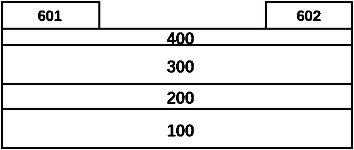
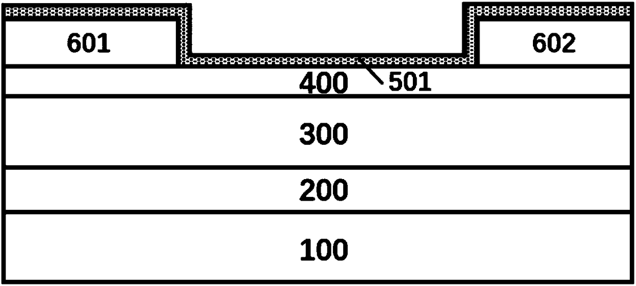
[0038] The device structure finally prepared by the method for manufacturing an enhancement mode gallium nitride field effect device according to an embodiment of the present invention. Such as Figure 7 As shown, the enhanced gallium nitride field effect device is mainly composed of the following parts: single crystal substrate 100, buffer layer 200, channel layer 300, barrier layer 400, two-dimensional material gate 501, source and drain metal electrodes 601 / 602 , a W gate metal electrode 603 , and a dielectric passivation layer 701 .

[0039] Figure 1 to Figure 7 It is a schematic diagram of the device structure according to various implementation steps of the manufacturing method of the enhancement mode GaN ...


PUM


Abstract

The invention provides a method for preparing an enhanced GaN field effect device structure. By inserting a layer of P-type two-dimensional semiconductor material under a gate metal, two-dimensional electron gas in a channel under a gate can be effectively depleted, and thus an enhanced GaN field effect device is prepared. The P-type two-dimensional semiconductor material of a contact region outside the lower part of the gate is etched and removed by using oxygen plasma, the contact resistance can be effectively reduced, and the device performance is improved. At the same time, by controllingan etching time and oxygen plasma concentration, an oxide film can be formed by a potential barrier layer by using the oxygen plasma, and the gate leakage of the device is reduced.

Description

technical field [0001] The invention relates to the field of manufacturing semiconductor devices, in particular to a method for preparing an enhanced gallium nitride field effect device. Background technique [0002] GaN materials have the characteristics of large band gap, high critical breakdown electric field, and high thermal conductivity, and have broad application prospects in broadband communications, power electronics, and other fields. [0003] Due to the spontaneous polarization and piezoelectric polarization effects at the interface between gallium nitride (GaN) and aluminum gallium nitride (AlGaN) heterojunction, the two-dimensional electron gas concentration is very high (>1E13cm -2 ), which makes GaN FETs [here FETs refer to HEMT (High Electron Mobility Transistor) devices] have very low on-resistance and switching delay. However, the high concentration of two-dimensional electron gas at the AlGaN / GaN heterointerface makes GaN FETs usually depletion-mode de...

Claims


Application Information

Patent Timeline
Patent Type & Authority Applications(China)
IPC IPC(8): H01L21/335H01L29/778
CPCH01L29/66462H01L29/7786
Inventor 梁世博
Owner BEIJING HUATAN TECH CO LTD
Why Eureka
Try Eureka