Nitride semiconductor microcavity laser structure capable of achieving electric injection maser and preparation method thereof
A nitride semiconductor, laser technology, applied in semiconductor lasers, lasers, laser parts and other directions, can solve problems such as increasing the optical loss of lasers
- Summary
- Abstract
- Description
- Claims
- Application Information
AI Technical Summary
Problems solved by technology
Method used
Image

Examples
Embodiment 1
[0067] Embodiment 1: Using technical solution 1 to manufacture a GaN self-supporting substrate blue microcavity laser.
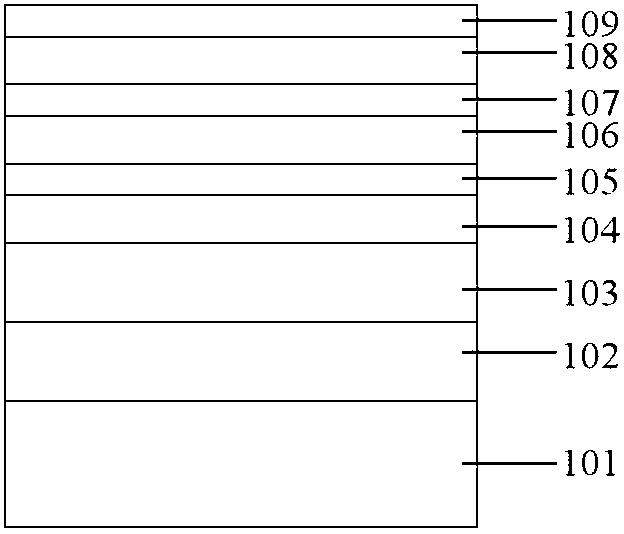
[0068] S1: GaN-based blue microcavity laser structures were grown on GaN free-standing substrates using metal-organic chemical vapor deposition (MOCVD), including 1500nm n-GaN contact layers, 130 pairs of n-Al 0.16 Ga 0.84 N / GaN superlattice structure, where each layer is 2.5nm thick as the lower optical confinement layer, 100nm n-In 0.03 Ga 0.97 N lower waveguide layer, 3 pairs of In 0.16 Ga 0.84 N / GaN multiple quantum wells, where each layer of In 0.16 Ga 0.84 N quantum well 2.5nm, each layer of GaN barrier 15nm, 80nm unintentionally doped In 0.03 Ga 0.97 Waveguide layer on N, 20nm p-Al 0.2 Ga 0.8 N electron blocking layer, 100 pairs of p-Al 0.16 Ga 0.84 N / GaN superlattice structure, where each layer is 2.5nm thick as the upper optical confinement layer, and a 30nm p-GaN contact layer, such as figure 1 shown.
[0069] S2: Clean the epitaxial waf...
Embodiment 2
[0074] Embodiment 2: adopting technical scheme 2 to manufacture a GaN-based violet microcavity laser on a Si substrate.
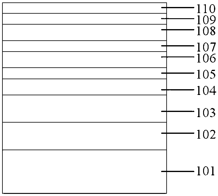
[0075] S1: Using metal organic chemical vapor deposition (MOCVD) equipment to grow a violet microcavity laser structure on a Si substrate, including a 2500nm n-GaN contact layer, 150 pairs of n-Al 0.2 Ga 0.8 N / GaN superlattice structure, where each layer is 3nm thick as the lower optical confinement layer, 100nm n-GaN lower waveguide layer, 3 pairs of In 0.1 Ga 0.9 N / GaN multiple quantum wells, where each layer of In 0.1 Ga 0.9 N quantum well 3nm, each layer of GaN barrier 10nm, 100nm unintentionally doped GaN upper waveguide layer, 20nm p-Al 0.25 Ga 0.75 N electron blocking layer, 100 pairs of p-Al 0.2 Ga 0.8 N / GaN superlattice structure, where each layer thickness is 3nm, as the upper optical confinement layer, 20nm p-GaN contact layer, such as Figure 6 shown.
[0076] S2: Clean the epitaxial wafer with acetone, alcohol, hydrochloric acid and de...
Embodiment 3
[0083] Embodiment 3: adopt technical scheme 3 to manufacture a GaN-based green microcavity laser on a sapphire substrate.
[0084] S1: A GaN-based green microcavity laser structure was grown on a sapphire substrate by metal-organic chemical vapor deposition (MOCVD), including a 500nm n-GaN contact layer, a 500nm heavily doped n-GaN layer, and a 100nm n-In 0.06 Ga 0.94 N lower waveguide layer, 3 pairs of In 0.3 Ga 0.7 N / GaN multiple quantum wells, where each layer of In 0.3 Ga 0.7 N quantum well 2nm, each layer of GaN barrier 8nm, 80nm unintentionally doped In 0.06 Ga 0.94 Waveguide layer on N, 20nm p-Al 0.2 Ga 0.8 N electron blocking layer, 20nm p-GaN contact layer, such as Figure 12 shown.
[0085] S2: Clean the epitaxial wafer with acetone, alcohol, hydrochloric acid and deionized water, deposit 350nm ITO, 50nm Cr and 100nm Au on the p-GaN contact layer in sequence, and anneal at 550°C in a compressed air atmosphere using a rapid annealing furnace 8 minutes to for...
PUM
| Property | Measurement | Unit |
|---|---|---|
| Size | aaaaa | aaaaa |
Abstract
Description
Claims
Application Information
 - R&D
- Intellectual Property
- Life Sciences
- Materials
- Tech Scout
- Unparalleled Data Quality
- Higher Quality Content
- 60% Fewer Hallucinations
Browse by: Latest US Patents, China's latest patents, Technical Efficacy Thesaurus, Application Domain, Technology Topic, Popular Technical Reports.
© 2025 PatSnap. All rights reserved.Legal|Privacy policy|Modern Slavery Act Transparency Statement|Sitemap|About US| Contact US: help@patsnap.com