A low-resistance, low-thermal-resistance nitride semiconductor microcavity laser structure and preparation method thereof

A nitride semiconductor and laser technology, used in semiconductor lasers, lasers, laser parts and other directions, can solve the problems affecting device reliability, large thermal resistance of devices, and increased optical loss, and achieve improved performance and reliability, heat conduction. The effect of short paths and reduced series resistance

Active Publication Date: 2021-07-06
江西省纳米技术研究院 +1
View PDF9 Cites 0 Cited by
  • Summary
  • Abstract
  • Description
  • Claims
  • Application Information

AI Technical Summary

Problems solved by technology

Not only that, the contact electrode will also affect the light field distribution inside the laser, resulting in an asymmetrical light field distribution, resulting in a decrease in the optical confinement factor of the microcavity laser, an increase in optical loss, and the inability of the microcavity laser to lase
[0010] Second, the existing nitride semiconductor microcavity lasers have a large resistance
However, the p-type layer in the laser is relatively thick, so the series resistance in the device is very large, causing a large amount of electric power to be converted into Joule heat, causing the junction temperature to rise, and affecting the performance and life of the device
In addition, for the existing Si substrate nitride microcavity laser, due to the "mushroom" structure, the n-electrode must be made on the Si substrate, and the current injection needs to pass through the Si substrate. However, there is a gap between the Si substrate and the GaN material. Non-doped, high-resistance AlN / AlGaN (AlN: 6.2eV, GaN: 3.4eV) buffer layer, so the resistance of the device is very large, and it is even more impossible to achieve electrical injection lasing
[0011] Third, the thermal resistance of existing nitride semiconductor microcavity lasers is very high, and the junction temperature of the active region is very high when the device is working, which seriously affects the device performance and life of the microcavity laser.
For nitride microcavity lasers with a "mushroom" structure, the InGaN / InGaN superlattice sacrificial layer or Si substrate at the edge has been removed, and when the microcavity laser is working, the edge area of ​​the device is the main propagation area of ​​the optical field, and the Generates a lot of heat that cannot be conducted directly down to the heat sink, resulting in a high thermal resistance of the device
For the nitride suspended film microcavity structure, as shown in the patent CN 104009393A, since the bottom of the microcavity laser is suspended, a large amount of heat generated by the laser cannot be conducted in time, resulting in a large thermal resistance of the device and a high junction temperature during operation, which not only affects the performance of the laser The internal quantum efficiency and threshold current will also seriously affect the reliability of the device
In addition, traditional nitride semiconductor microcavity lasers are packaged in a front-mounted way, and the heat needs to be conducted to the heat sink through a laser structure with a thickness of about 3 μm and a substrate with a thickness of about 100 μm. The heat conduction path of the laser is very long, and because the substrate Low thermal conductivity, resulting in high thermal resistance of the laser
However, the thermal power of the laser is large, so the junction temperature of the device is high, which seriously affects the performance and life of the device.
[0012] Fourth, the stability of existing nitride semiconductor microcavity lasers is very poor, and it is difficult to be practically applied
For nitride microcavity lasers with a "mushroom" structure, the InGaN / InGaN superlattice sacrificial layer or Si substrate at the edge has been removed, and the device is only supported by a small pillar in the middle of the bottom of the microcavity laser. Due to the small size of the pillars, Therefore, the mechanical support strength and stability of the device are poor
For the nitride suspended film microcavity structure, because the bottom of the microcavity laser is suspended, the mechanical support strength and stability of this device are worse
In addition, because the (0001) gallium surface nitride semiconductor has good chemical stability and is not easy to corrode, dry etching is usually used to make the sidewall of the microcavity laser. Dry etching will not only lead to rough sidewalls, but also cause light scattering, etc.
Dry etching will also introduce surface states, damages and defects, these surface states, damages and defects will not only become non-radiative recombination centers, affecting the efficiency of microcavity lasers; they will also become leakage channels, affecting the reliability and stability of devices
[0013] Fifth, the preparation process of the existing nitride semiconductor microcavity laser is complicated, and it is difficult to ensure the consistency and repeatability of the device
This "mushroom" structure nitride microcavity laser cavity has a low-quality and high-dislocation defect-density AlN / AlGaN buffer layer inside, and these low-quality and high-defect-density buffer layers will produce strong light absorption or non-radiative recombination , increasing the optical loss of the laser

Method used


Image

  • A low-resistance, low-thermal-resistance nitride semiconductor microcavity laser structure and preparation method thereof
  • A low-resistance, low-thermal-resistance nitride semiconductor microcavity laser structure and preparation method thereof
  • A low-resistance, low-thermal-resistance nitride semiconductor microcavity laser structure and preparation method thereof

Examples


Embodiment 1

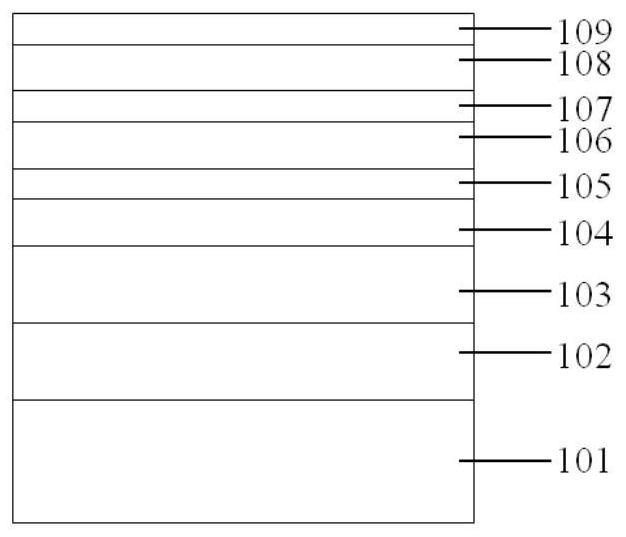
[0094] Embodiment 1 is used to fabricate a GaN-based blue microcavity laser on a Si substrate.

[0095] S1: A GaN-based blue microcavity laser structure was grown on a Si substrate by metal-organic chemical vapor deposition (MOCVD), including a 1500nm n-GaN contact layer, 100 pairs of n-Al 0.16 Ga 0.84 N / GaN superlattice structure, where each layer is 2.5nm thick, as n-type optical confinement layer, 100nm n-In 0.03 Ga 0.97 N lower waveguide layer, 3 pairs of In 0.16 Ga 0.84 N / GaN multiple quantum wells, where each layer of In 0.16 Ga 0.84 N quantum well 2.5nm, each layer of GaN barrier 15nm, 80nm unintentionally doped In 0.03 Ga 0.97 Waveguide layer on N, 20nm p-Al 0.2 Ga 0.8 N electron blocking layer, 100 pairs of p-Al 0.16 Ga 0.84 N / GaN superlattice structure, where each layer has a thickness of 2.5nm as the upper optical confinement layer, and a 30nm p-GaN contact layer, such as figure 1 shown.

[0096] S2: Clean the epitaxial wafer with acetone, alcohol, hydr...

Embodiment 2

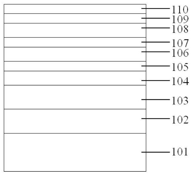
[0105] A GaN self-supporting substrate near-ultraviolet microcavity laser is fabricated by adopting the second embodiment.

[0106] S1: Growth of a near-ultraviolet microcavity laser structure on a GaN free-standing substrate using metal-organic chemical vapor deposition (MOCVD) equipment, including a 2500nm n-AlGaN contact layer, 100 pairs of n-Al 0.2 Ga 0.8 N / GaN superlattice structure, in which each layer is 3nm thick, as n-type optical confinement layer, 120nm n-GaN lower waveguide layer, 3 pairs of In 0.03 Ga 0.97 N / AlGaN multiple quantum wells, where each layer of In 0.03 Ga 0.97 N quantum well 3nm, each layer of AlGaN barrier 10nm, 100nm unintentionally doped GaN upper waveguide layer, 20nm p-Al 0.25 Ga 0.75 N electron blocking layer, 100 pairs of p-Al 0.2 Ga 0.8 N / GaN superlattice structure, where each layer thickness is 3nm, as the upper optical confinement layer, 20nm p-GaN contact layer, such as Figure 8 shown.

[0107] S2: Clean the epitaxial wafer with a...

Embodiment 3

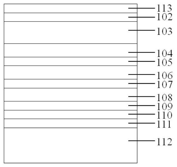
[0118] A GaN-based green microcavity laser on a sapphire substrate is manufactured using Embodiment 3.

[0119] S1: Grow a GaN-based green microcavity laser structure on a sapphire substrate using metal-organic chemical vapor deposition (MOCVD), including a 500nm n-GaN contact layer, a 500nm heavily doped n-GaN layer, and a 100nm n-In 0.06 Ga 0.94 N lower waveguide layer, 3 pairs of In 0.3 Ga 0.7 N / GaN multiple quantum wells, where each layer of In 0.3 Ga 0.7 N quantum well 2nm, each layer of GaN barrier 8nm, 80nm unintentionally doped In 0.06 Ga 0.94 Waveguiding layer on N, 20nm p-Al 0.2 Ga 0.8 N electron blocking layer, 20nm p-GaN contact layer, such as Figure 16 shown.

[0120] S2: Clean the epitaxial wafer with acetone, alcohol, hydrochloric acid and deionized water, etc., deposit 350nm ITO, 50nm Cr and 100nm Au on the p-GaN contact layer in sequence, and use a rapid annealing furnace at 550°C in a compressed air atmosphere Anneal for 8 minutes to form a good oh...


PUM

PropertyMeasurementUnit
sizeaaaaaaaaaa
thicknessaaaaaaaaaa
thicknessaaaaaaaaaa

Abstract

The invention provides a semiconductor microcavity laser structure and a preparation method thereof. The microcavity laser is prepared on the nitrogen surface of the nitride semiconductor, and the p-type ohmic contact of the (0001) gallium surface adopts the whole-surface contact method, which greatly reduces the cost of the microcavity laser. The series resistance of the microcavity laser; the heat of the microcavity laser is directly conducted to the heat sink with high thermal conductivity, and the microcavity laser is prepared on the nitrogen surface, and the side wall of the microcavity laser is fabricated by wet etching, which can greatly improve the stability of the microcavity laser properties, using AlInGaN, ITO, AZO, IGZO, porous GaN, Ag, Al, ZnO, MgO, Si, SiO 2 , SiNx, TiO 2 , ZrO 2 , AlN, Al 2 o 3 、 Ta 2 o 5 , HfO 2 , HfSiO 4 , AlON material is used as the optical confinement layer of the microcavity laser to provide strong optical confinement. The novel nitride semiconductor microcavity laser structure proposed by the present invention has the advantages of small resistance, low thermal resistance, easy implementation of electric injection, good stability and reliability, etc., and can greatly enhance the performance and service life of the nitride semiconductor microcavity laser.

Description

technical field [0001] The present invention relates to a low-resistance, low-thermal-resistance nitride semiconductor microcavity laser structure and a preparation method thereof, in particular to a III-V group nitride semiconductor microcavity with low resistance, low thermal resistance and easy electrical injection lasing The laser structure and its preparation method belong to the field of semiconductor optoelectronic technology. Background technique [0002] III-V nitride semiconductors are called third-generation semiconductor materials, which have the advantages of large bandgap, good chemical stability, and strong radiation resistance; their bandgap covers from deep ultraviolet, the entire visible light, to near-infrared range, can be used to make light-emitting diodes and lasers, etc. The Whispering-gallery Mode microcavity laser has the advantages of small mode volume, high quality factor, and low threshold. Microcavity lasers based on III-V nitride semiconductor...

Claims


Application Information

Patent Timeline
Patent Type & Authority Patents(China)
IPC IPC(8): H01S5/042H01S5/32
CPCH01S5/0421H01S5/32
Inventor 孙钱冯美鑫周宇高宏伟杨辉
Owner 江西省纳米技术研究院
Why Eureka
Try Eureka