Nitride semiconductor microcavity laser structure with low electric resistance and low thermal resistance
A nitride semiconductor and laser technology, used in semiconductor lasers, lasers, laser parts, etc., can solve the problems affecting the device performance and life of microcavity lasers, the inability of heat to be conducted in time, and the increase of laser light loss.
- Summary
- Abstract
- Description
- Claims
- Application Information
AI Technical Summary
Problems solved by technology
Method used
Image
Examples
Embodiment 1
[0094] Embodiment 1 is used to fabricate a GaN-based blue microcavity laser on a Si substrate.
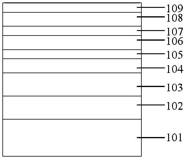
[0095] S1: A GaN-based blue microcavity laser structure was grown on a Si substrate by metal-organic chemical vapor deposition (MOCVD), including a 1500nm n-GaN contact layer, 100 pairs of n-Al 0.16 Ga 0.84 N / GaN superlattice structure, where each layer is 2.5nm thick, as n-type optical confinement layer, 100nm n-In 0.03 Ga 0.97 N lower waveguide layer, 3 pairs of In 0.16 Ga 0.84 N / GaN multiple quantum wells, where each layer of In 0.16 Ga 0.84 N quantum well 2.5nm, each layer of GaN barrier 15nm, 80nm unintentionally doped In 0.03 Ga 0.97 Waveguide layer on N, 20nm p-Al 0.2 Ga 0.8 N electron blocking layer, 100 pairs of p-Al 0.16 Ga 0.84 N / GaN superlattice structure, where each layer has a thickness of 2.5nm as the upper optical confinement layer, and a 30nm p-GaN contact layer, such as figure 1 shown.
[0096] S2: Clean the epitaxial wafer with acetone, alcohol, hydr...
Embodiment 2
[0105] A GaN self-supporting substrate near-ultraviolet microcavity laser is fabricated by adopting the second embodiment.
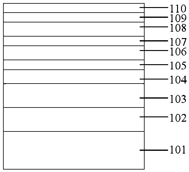
[0106] S1: Growth of a near-ultraviolet microcavity laser structure on a GaN free-standing substrate using metal-organic chemical vapor deposition (MOCVD) equipment, including a 2500nm n-AlGaN contact layer, 100 pairs of n-Al 0.2 Ga 0.8 N / GaN superlattice structure, in which each layer is 3nm thick, as n-type optical confinement layer, 120nm n-GaN lower waveguide layer, 3 pairs of In 0.03 Ga 0.97 N / AlGaN multiple quantum wells, where each layer of In 0.03 Ga 0.97 N quantum well 3nm, each layer of AlGaN barrier 10nm, 100nm unintentionally doped GaN upper waveguide layer, 20nm p-Al 0.25 Ga 0.75 N electron blocking layer, 100 pairs of p-Al 0.2 Ga 0.8 N / GaN superlattice structure, where each layer thickness is 3nm, as the upper optical confinement layer, 20nm p-GaN contact layer, such as Figure 8 shown.
[0107] S2: Clean the epitaxial wafer with a...
Embodiment 3
[0118] A GaN-based green microcavity laser on a sapphire substrate is manufactured using Embodiment 3.
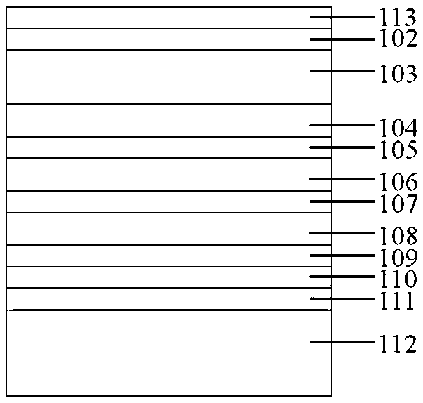
[0119] S1: Grow a GaN-based green microcavity laser structure on a sapphire substrate using metal-organic chemical vapor deposition (MOCVD), including a 500nm n-GaN contact layer, a 500nm heavily doped n-GaN layer, and a 100nm n-In 0.06 Ga 0.94 N lower waveguide layer, 3 pairs of In 0.3 Ga 0.7 N / GaN multiple quantum wells, where each layer of In 0.3 Ga 0.7 N quantum well 2nm, each layer of GaN barrier 8nm, 80nm unintentionally doped In 0.06 Ga 0.94 Waveguiding layer on N, 20nm p-Al 0.2 Ga 0.8 N electron blocking layer, 20nm p-GaN contact layer, such as Figure 16 shown.
[0120] S2: Clean the epitaxial wafer with acetone, alcohol, hydrochloric acid and deionized water, etc., deposit 350nm ITO, 50nm Cr and 100nm Au on the p-GaN contact layer in sequence, and use a rapid annealing furnace at 550°C in a compressed air atmosphere Anneal for 8 minutes to form a good oh...
PUM
| Property | Measurement | Unit |
|---|---|---|
| Size | aaaaa | aaaaa |
| Thickness | aaaaa | aaaaa |
| Thickness | aaaaa | aaaaa |
Abstract
Description
Claims
Application Information


