
Ultra-efficient organic electroluminescent diode device

A luminescence and diode technology, applied in the field of ultra-high-efficiency organic electroluminescent diode devices, can solve the problems of external quantum efficiency, power efficiency roll-off, high turn-on and operating voltage, and limited material selection, so as to reduce the external quantum efficiency of the device and Roll-off of power efficiency, reduction of turn-on and operating voltages, effects of lower selection requirements

Active Publication Date: 2018-08-03
SUZHOU UNIV
View PDF5 Cites 10 Cited by
  • Summary
  • Abstract
  • Description
  • Claims
  • Application Information

AI Technical Summary

Problems solved by technology

[0004] Technical problems to be solved: A series of problems existing in the preparation of exciplex-based high-efficiency organic light-emitting diodes (OLEDs) devices: (1) current high-efficiency organic light-emitting diode devices based on exciplexes The medium donor material (Donor) needs to meet stringent requirements, such as the deep highest occupied molecular orbital (HOMO) energy level, which greatly limits the choice of materials; In light-emitting diode devices, due to the need to meet the emission of blue light, the formed exciplexes have a higher band gap, resulting in higher turn-on and operating voltages; (3) the current high-efficiency organic electroluminescence based on exciplexes Diode devices have serious roll-offs in external quantum efficiency and power efficiency at high operating brightness; (4) At present, high-efficiency organic electroluminescent diode devices based on exciplexes have poor spectral stability under different operating brightness. have a large drift

Method used


Image

  • Ultra-efficient organic electroluminescent diode device
  • Ultra-efficient organic electroluminescent diode device
  • Ultra-efficient organic electroluminescent diode device

Examples


Embodiment 1

[0046] A method for preparing an ultra-high-efficiency organic electroluminescent diode device, comprising the following steps:

[0047] (1) Clean the indium tin oxide (ITO) transparent conductive glass substrate with acetone, ethanol and deionized water for three times, and then move it to a 105°C oven to completely remove the residual solvent and water on the surface;

[0048] (2) After taking out the ITO transparent conductive glass substrate, treat it with ultraviolet lamp and ozone for 15 minutes;

[0049] (3) Take it out, place it in a vacuum film deposition chamber, and vacuum it to 5.0×10 -4 Torr;

[0050] (4) Vacuum-evaporate HAT-CN on the processed ITO to form a hole injection layer, the evaporation rate is 0.4 Å / s, and the evaporation thickness is 10 nm;

[0051] (5) Continue to vacuum-evaporate TAPC on the ITO substrate on which the HAT-CN was evaporated to form a hole transport layer. The evaporation rate is 2 Å / s and the evaporation thickness is 40 nm;

[005...

Embodiment 2

[0060] A method for preparing an ultra-high-efficiency organic electroluminescent diode device, comprising the following steps:

[0061] (1) Clean the indium tin oxide (ITO) transparent conductive glass substrate with acetone, ethanol and deionized water for three times, and then move it to a 105°C oven to completely remove the residual solvent and water on the surface;

[0062] (2) After taking out the ITO transparent conductive glass substrate, treat it with ultraviolet lamp and ozone for 15 minutes;

[0063] (3) Take it out, put it in the vacuum film deposition chamber, and vacuum it to 6.0×10 -6 Torr;

[0064] (4) Vacuum-evaporate HAT-CN on the processed ITO to form a hole injection layer, the evaporation rate is 0.4 Å / s, and the evaporation thickness is 10 nm;

[0065] (5) Continue to vacuum-evaporate TAPC on the ITO substrate on which the HAT-CN was evaporated to form a hole transport layer. The evaporation rate is 2 Å / s and the evaporation thickness is 40 nm;

[006...

Embodiment 3

[0074] A method for preparing an ultra-high-efficiency organic electroluminescent diode device, comprising the following steps:

[0075] (1) Clean the indium tin oxide (ITO) transparent conductive glass substrate with acetone, ethanol and deionized water for three times, and then move it to a 105°C oven to completely remove the residual solvent and water on the surface;

[0076] (2) After taking out the ITO transparent conductive glass substrate, treat it with ultraviolet lamp and ozone for 15 minutes;

[0077] (3) Take it out, place it in a vacuum film deposition chamber, and vacuum it to 5.0×10 -6 Torr;

[0078] (4) Vacuum-evaporate HAT-CN on the processed ITO to form a hole injection layer, the evaporation rate is 0.4 Å / s, and the evaporation thickness is 10 nm;

[0079](5) Continue to vacuum-evaporate TAPC on the ITO substrate on which the HAT-CN was evaporated to form a hole transport layer. The evaporation rate is 2 Å / s and the evaporation thickness is 40 nm;

[0080...


PUM

PropertyMeasurementUnit
Thicknessaaaaaaaaaa

Abstract

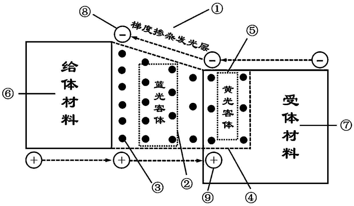
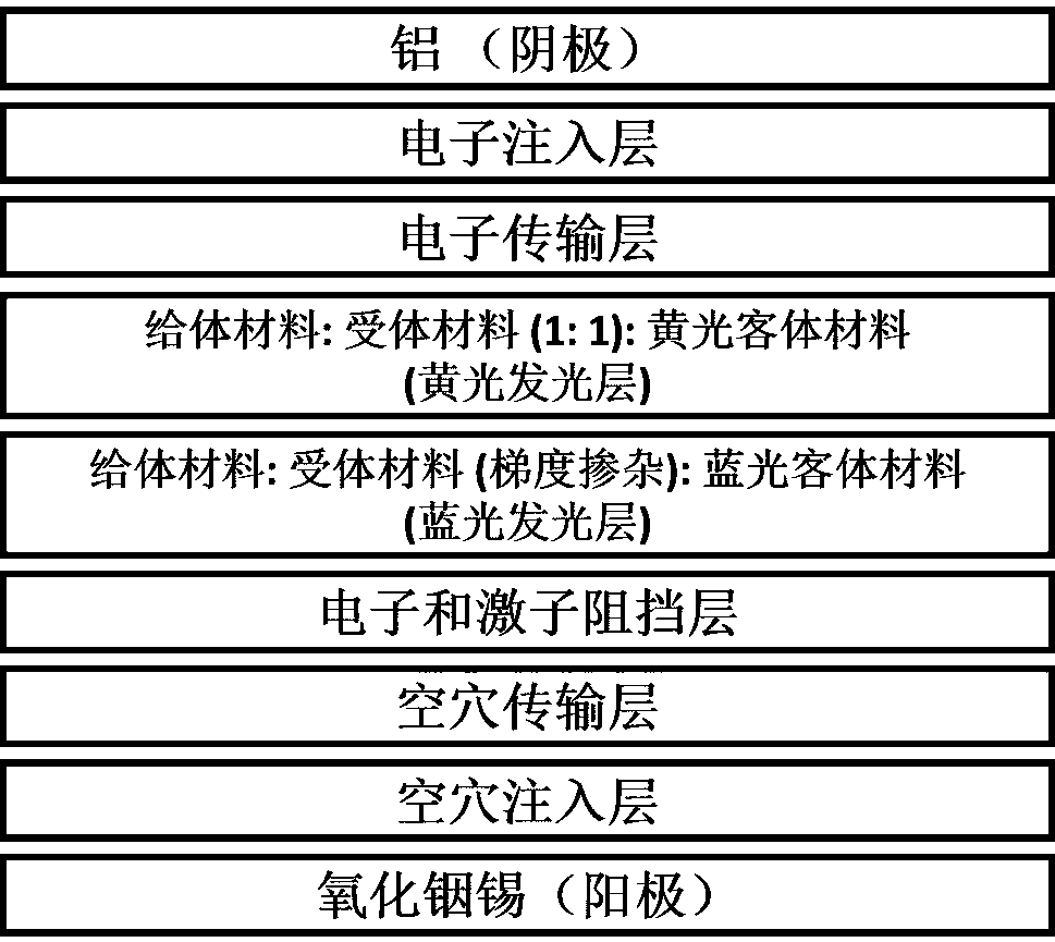
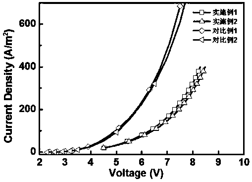
The invention provides an ultra-efficient organic electroluminescent diode device which comprises a gradient-doped double-body light-emitting layer. The double-body light-emitting layer comprises a single-band light-emitting layer or a multi-band light-emitting layer. The light-emitting form comprises fluorescence, phosphorescence or heat excitation delayed fluorescent luminescence. The device further comprises a transparent conductive glass substrate, a hole injection layer, a hole transport layer, an electron and exciton blocking layer, an electron transport layer, an electron injection layer or a metal cathode electrode. The method greatly reduces the selection requirement of a donor material, and improves the universality of the donor material. A formed exciplex can excite the long-wavelength donor material, and can prepare an efficient multi-band device. Through the structure design of the gradient-doped light-emitting layer, the start and working voltage of the device can be reduced. A widened exciton composite region effectively reduces the roll-off of the current efficiency and power efficiency of the device under high brightness. The spectral stability of single-band and multi-band devices is greatly improved under different working brightness.

Description

technical field [0001] The invention belongs to the field of organic light-emitting semiconductor devices, and in particular relates to an ultra-high-efficiency organic light-emitting diode device. Background technique [0002] White organic light-emitting diodes (WOLEDs) are being hailed as the next generation of solid-state display and lighting technologies. Currently, WOLED technology has been applied in smart phones, smart watches, MP3 and flat-panel TVs. Moreover, it has also received extensive attention in the field of lighting. [0003] WOLED is a self-luminous device. Usually, the structure of the device is an organic functional layer sandwiched between a transparent anode and a metal cathode electrode. By applying an external voltage, electrons and holes are injected from the metal cathode and transparent anode respectively. The transport layer recombines in the light-emitting layer to form excitons that emit visible light when returning to the ground state by rad...

Claims


Application Information

Patent Timeline
IPC IPC(8): H01L51/50H01L51/56
CPCH10K50/12H10K50/13H10K71/00
Inventor 廖良生蒋佐权汤洵
Owner SUZHOU UNIV
Learn More