
Method for constructing nano coating on surface of micro-nano structure and application of nano coating on antireflection

A nano-coating and micron-level technology, applied in coatings, electrical components, circuits, etc., can solve the problems of low solar energy utilization, and achieve the effect of facilitating large-scale preparation, improving transmittance, and requiring simple equipment

Active Publication Date: 2018-08-07
INST OF CHEM CHINESE ACAD OF SCI
View PDF2 Cites 8 Cited by
  • Summary
  • Abstract
  • Description
  • Claims
  • Application Information

AI Technical Summary

Problems solved by technology

At present, the methods for constructing nano-coatings include layer-by-layer self-assembly technology, nano-lithography technology, nano-imprinting technology, etc. However, most of these methods are aimed at the construction of nano-coatings on flat and smooth surfaces, and the construction of nano-coatings on irregular surfaces layers are rarely reported
[0003] Solar energy is widely used as a clean and renewable energy source. However, due to the limitation of solar cell materials or components, the utilization rate of solar energy is low. Therefore, anti-reflection treatment of solar cell packaging materials is an effective Ways to Improve Solar Energy Utilization Efficiency
At present, on the surface of flat optical materials, the preparation of anti-reflection films has a solid research foundation and technology accumulation. However, on the surface of optical materials with micro-nano structures, such as liquid crystal display backlight systems, Fresnel lenses, solar cells, etc. There are few reports on the construction of anti-reflection coatings with crystalline silicon, etc.

Method used


Image

  • Method for constructing nano coating on surface of micro-nano structure and application of nano coating on antireflection
  • Method for constructing nano coating on surface of micro-nano structure and application of nano coating on antireflection
  • Method for constructing nano coating on surface of micro-nano structure and application of nano coating on antireflection

Examples


Embodiment 1

[0072] 1) Dilute γ-aminopropyltriethoxysilane and ethanol at a volume ratio of 1:10 to obtain solution a;

[0073] 2) Dilute the dispersion of silicon dioxide nanoparticles (~30nm, negatively charged) with a mass fraction of 60% and ethanol at a volume ratio of 1:10 to obtain solution b; take 30 μL of solution a and drop it into 30 ml of solution b, that is obtaining nanoparticle coatings;

[0074] 3) At 80°C, vapor-phase deposit 1mL of solution a onto the surface of a silicon wafer with an irregular micron-scale structure;

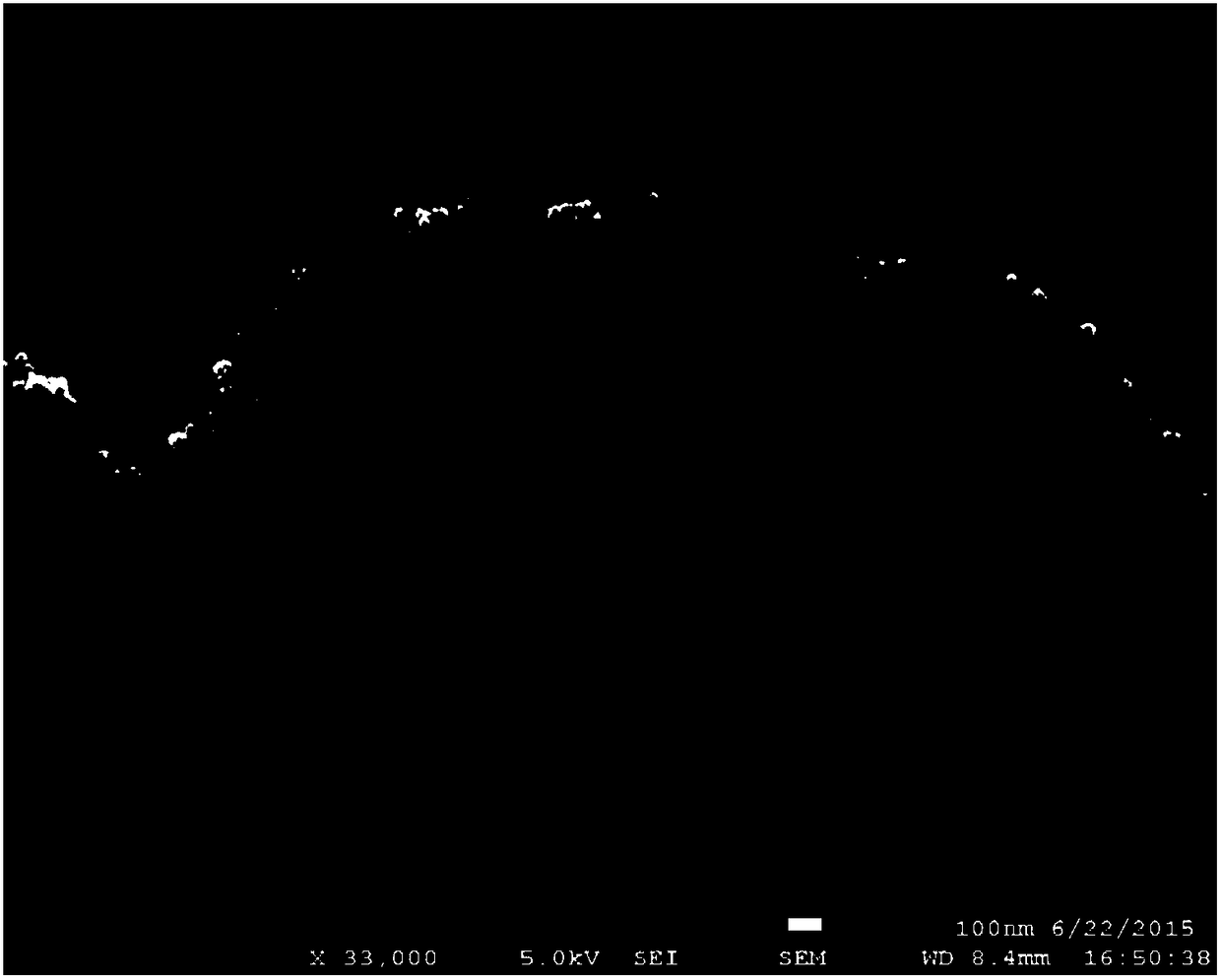
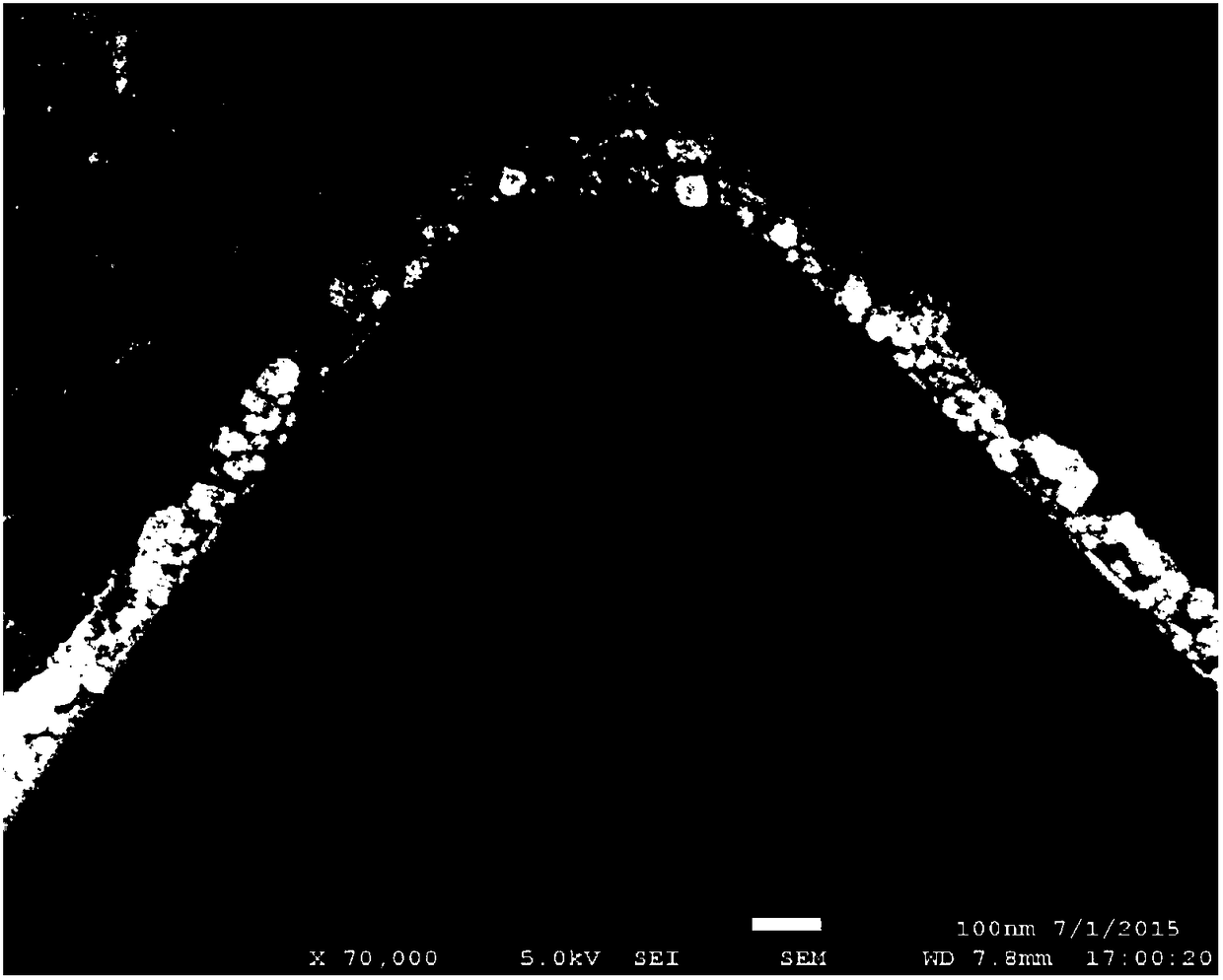
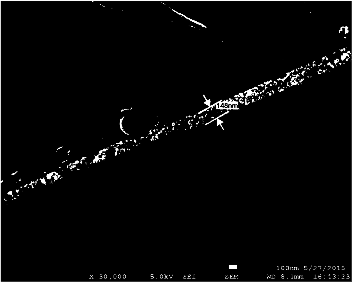
[0075] 4) At room temperature, after immersing the silicon chip of vapor deposition solution a in step (3) in the nanoparticle coating described in step (2) for 8 hours, take it out, rinse the surface with ethanol, and after drying at room temperature, irregular micron-sized A conformal, uniform thickness (approximately 150 nm) coating of silica nanoparticles was formed on the surface of the structured silicon wafer.

[0076] If the immersion time in st...

Embodiment 2

[0078] 1) Dilute γ-aminopropyltriethoxysilane and ethanol at a volume ratio of 1:100 to obtain solution a;

[0079] 2) Dilute the dispersion of silicon dioxide nanoparticles (~30nm, negatively charged) with a mass fraction of 60% and ethanol at a volume ratio of 1:100 to obtain solution b; take 300 μL of solution a and drop it into 30ml of solution b, that is obtaining nanoparticle coatings;

[0080] 3) At 80°C, vapor-phase deposit 10mL of solution a onto the surface of a silicon wafer with an irregular micron-scale structure;

[0081] 4) At room temperature, after immersing the silicon chip of vapor deposition solution a in step (3) in the nanoparticle coating described in step (2) for 10 h, take it out, rinse the surface with ethanol, and dry it at room temperature to have irregular micron-scale A conformal, uniform thickness (approximately 200 nm) coating of silica nanoparticles was formed on the surface of the structured silicon wafer.

[0082] If the immersion time of t...

Embodiment 3

[0084] 1) Dilute γ-aminopropyltriethoxysilane and ethanol at a volume ratio of 1:150 to obtain solution a;

[0085] 2) Dilute the dispersion of silicon dioxide nanoparticles (~30nm, negatively charged) with a mass fraction of 70% and ethanol at a volume ratio of 1:150 to obtain solution b; take 200 μL of solution a and drop it into 30ml of solution b, that is obtaining nanoparticle coatings;

[0086] 3) At 90°C, vapor deposition of 20 mL of solution a onto the surface of cicada wings with irregular nanoscale structures;

[0087] 4) At room temperature, after immersing the cicada wings of the vapor deposition solution a in step (3) in the nanoparticle coating described in step (2) for 10 hours, take it out, rinse the surface with ethanol, and dry at room temperature to have irregular nano-scale A conformal, uniform thickness (approximately 200 nm) coating of silica nanoparticles formed on the surface of the structured cicada wings.

[0088] If the immersion time of the cicada...


PUM

PropertyMeasurementUnit
Thicknessaaaaaaaaaa
Thicknessaaaaaaaaaa
Thicknessaaaaaaaaaa

Abstract

The invention discloses a method for constructing a nano coating on the surface of a micro-nano structure and application of the nano coating on antireflection. In the method, a nano-particle coatingis adopted and comprises a solution a and a solution b; the solution a comprises a silane coupling agent and a solvent; the solution b comprises nano-particle dispersion liquid and a solvent; the solution a is dropwise added in the solution b to obtain the nano-particle coating; and the silane coupling agent in the solution a has positive electricity, and nano-particles in the solution b has negative electricity or is improved by substances which have negative electricity. By the method, the conformal nano coating with the uniform thickness is constructed on the surface with an irregular micro-nano structure, and furthermore, the thickness of the coating can be regulated and controlled according to time of immersion in the nano-particle coating. In addition, the method for constructing thenano coating is applied to antireflection, and thus, a transmittance value of a substrate is increased to a certain extent on the original.

Description

technical field [0001] The invention relates to a method for constructing a conformal, uniform thickness and controllable nano-coating on the surface of a micro-nano structure and its application in anti-reflection, belonging to the technical field of surface treatment. Background technique [0002] With the rapid development of nanotechnology, nanomaterials have shown broad application prospects. Among them, nano-coating has been widely used in optoelectronic technology, conductor or semiconductor devices, sensors and so on. At present, the methods for constructing nano-coatings include layer-by-layer self-assembly technology, nano-lithography technology, nano-imprinting technology, etc. However, most of these methods are aimed at the construction of nano-coatings on flat and smooth surfaces, and the construction of nano-coatings on irregular surfaces layers are rarely reported. [0003] Solar energy is widely used as a clean and renewable energy source. However, due to t...

Claims


Application Information

Patent Timeline
IPC IPC(8): C09D1/00C09D7/63H01L31/0216
CPCC09D1/00H01L31/02168
Inventor 侯仪蔡超王真赵宁徐坚
Owner INST OF CHEM CHINESE ACAD OF SCI
Learn More