Grooved gate short circuit anode SOI LIGBT

A technology of slot grid and anode, which is applied in the direction of circuits, electrical components, semiconductor devices, etc., can solve the problems of large conduction voltage drop, low anode hole injection efficiency, and influence on the uniformity of device current distribution, etc., to reduce the conduction voltage The effect of reducing, eliminating the voltage foldback phenomenon, and eliminating the voltage foldback effect

Active Publication Date: 2018-08-10
UNIV OF ELECTRONICS SCI & TECH OF CHINA
View PDF4 Cites 14 Cited by
  • Summary
  • Abstract
  • Description
  • Claims
  • Application Information

AI Technical Summary

Problems solved by technology

However, the introduction of the short-circuited anode structure makes the device switch between unipolar and bipolar modes when it is turned on, which brings the voltage foldback effect to the device and affects the uniformity of the current distribution of the device.
At the same time, the introduction of the short-circuited anode structure will make the anode hole injection efficiency low and the conduction voltage drop large.

Method used


Image

  • Grooved gate short circuit anode SOI LIGBT
  • Grooved gate short circuit anode SOI LIGBT
  • Grooved gate short circuit anode SOI LIGBT

Examples


Embodiment 1

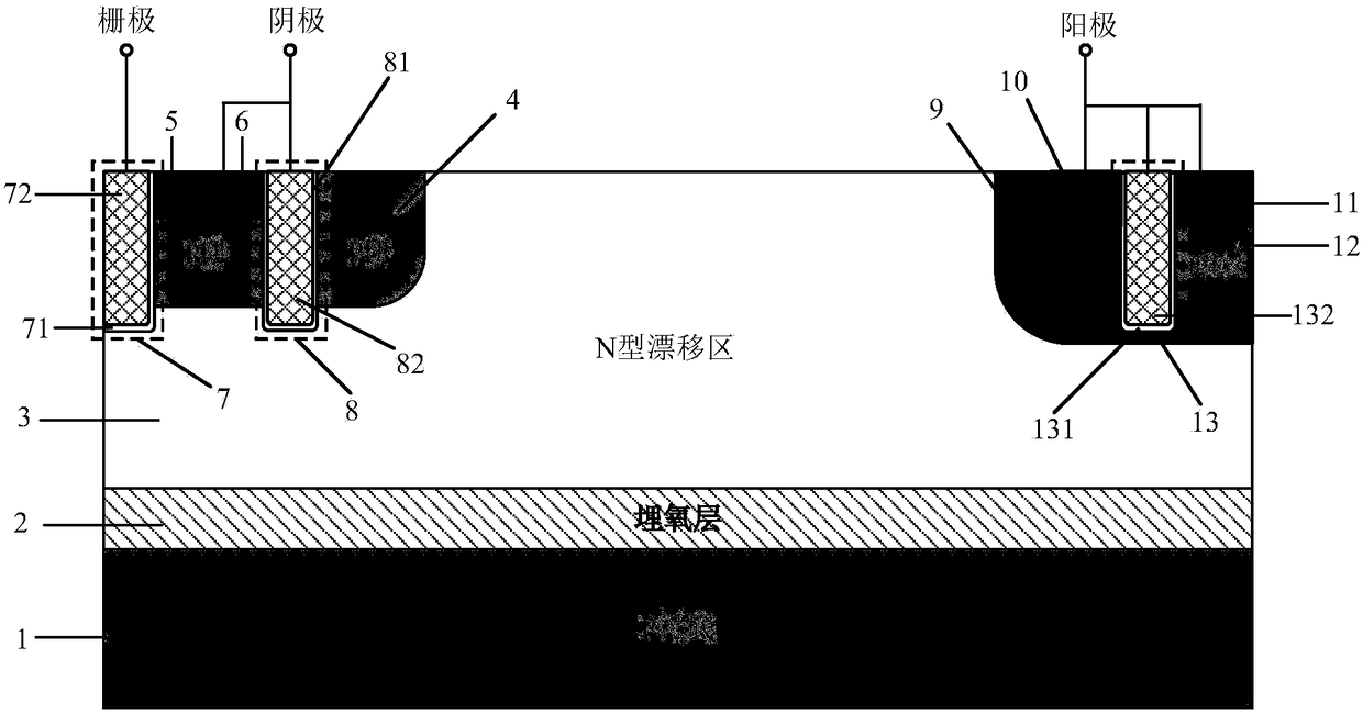
[0019] Such as figure 1 As shown, the SOI LIGBT of this example includes a P substrate 1, a buried oxide layer 2, and a top semiconductor layer stacked sequentially from bottom to top; the top semiconductor layer has an N-type drift region 3, and an N-type drift region 3 One side has a P well region 4, and the other side is an anode structure; the upper surface of the P well region 4 has an N+ cathode region 5 and a P+ body contact region 6, and the lead end of the P+ body contact region 6 is a cathode; In the well region 4, there are groove grids 7 and cathode grooves 8 that penetrate the P well region 4 from the surface and extend from the bottom to the N-type semiconductor drift region 3, and the groove grids 7 are in contact with the N+ cathode region 5, and the cathode grooves 8 In contact with the P+ body contact region 6, the slot grid 7 and the cathode slot 8 respectively have a first insulating dielectric layer 71 and a second insulating dielectric layer 81 located on...

Embodiment 2

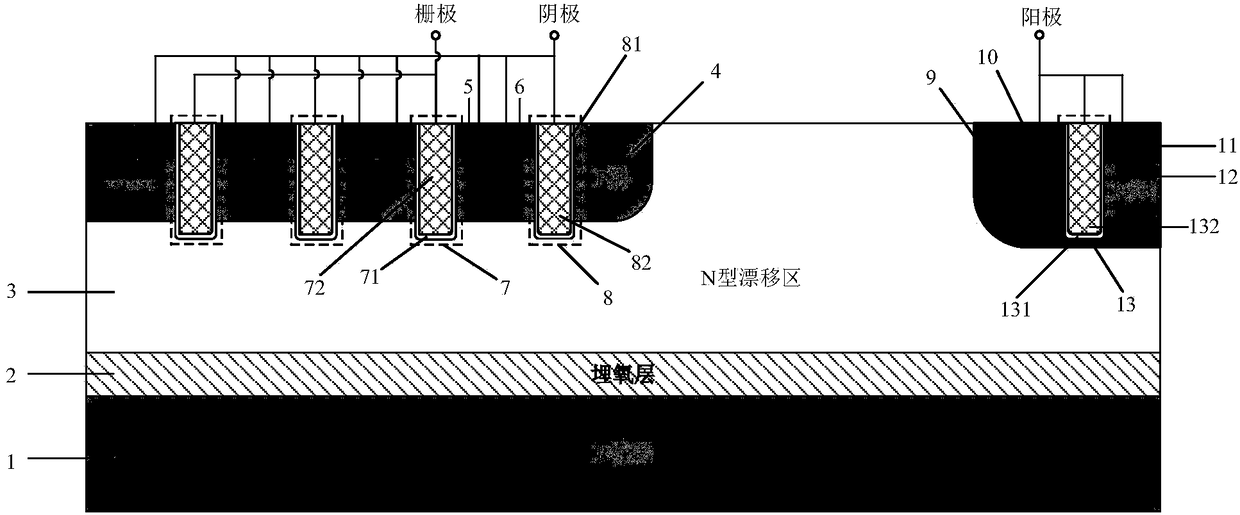
[0023] Such as figure 2 As shown, compared with Embodiment 1, there are multiple slot gates 7 and cathode slots 8 in this example, which are alternately arranged along the lateral direction of the device. Multiple trench gates increase the channel density of the device and reduce the conduction voltage drop.

Embodiment 3

[0025] Such as image 3 As shown, compared with Embodiment 2, the N+ cathode region 5 is connected to the cathode in this example.


PUM


Abstract

The invention belongs to the technical field of power semiconductors and relates to a grooved gate short circuit anode SOI LIGBT. In comparison with the traditional short circuit anode LIGBT, anode grooves connected to anode potential are introduced at an anode end, and a P body area is introduced right below an N+ anode area; and grooved gates and cathode grooves connected with a cathode are introduced in a cathode area. When the device is turned off, the anode groove is connected to high potential, an NMOS in the anode area is started automatically, extraction of electrons stored in a driftarea is quickened, and the turn-off time and the turn-off energy loss are reduced; when the device is in a high-voltage high-current state, the cathode groove forms a hole bypass, and happening of latch-up effects is suppressed; when the device is conducted, under blocking of an electronic barrier in the P body area, electron current in the drift region is not easy to be collected by the N+ anode,voltage reentry effects are eliminated, and as the grooved gate structures of the cathode are in parallel connection, the channel density is increased and the conduction voltage drop is reduced. Thegrooved gate short circuit anode SOI LIGBT has the beneficial effects that in comparison with the traditional short circuit anode LIGBT, a voltage reentry phenomenon is eliminated under a smaller transverse cell size, and the conduction voltage drop is lower.

Description

technical field [0001] The invention belongs to the technical field of power semiconductors, and relates to a slot-gate short-circuited anode SOI LIGBT (Lateral Insulated Gate Bipolar Transistor, lateral insulated gate bipolar transistor). Background technique [0002] IGBT is a new device combining MOSFET (Metal Oxide Semiconductor Field Effect Transistor) and BJT (Bipolar Junction Transistor). It not only has the advantages of high input impedance of MOSFET and low on-resistance of BJT, but also realizes High breakdown voltage and high forward current. Among them, lateral IGBT (LIGBT) is easy to be integrated in silicon-based, especially SOI-based power integrated circuits. SOI-based LIGBT can completely eliminate the hole-electron injection of bulk silicon LIGBT substrate, and the use of dielectric isolation SOI technology is easy to achieve device integration. Complete electrical isolation makes SOI LIGBT widely used in high-tech industries such as power electronics, in...

Claims


Application Information

Patent Timeline
Patent Type & Authority Applications(China)
IPC IPC(8): H01L29/739
CPCH01L29/7394
Inventor 罗小蓉赵哲言黄琳华邓高强孙涛张波
Owner UNIV OF ELECTRONICS SCI & TECH OF CHINA
Why Eureka
Try Eureka