Wafer-level heterogeneous integrated high-frequency system and manufacturing method thereof

A wafer-level, heterogeneous technology, applied in the field of microelectronics, can solve the problems of serious bonding loss and parasitic effects, unfavorable development of system miniaturization, and reduced overall system performance, so as to reduce the influence of parasitic effects and shorten the internal The effect of interconnection and risk reduction

Active Publication Date: 2020-01-14
XIDIAN UNIV
View PDF5 Cites 0 Cited by
  • Summary
  • Abstract
  • Description
  • Claims
  • Application Information

AI Technical Summary

Problems solved by technology

[0008] In the existing technology, limited by the current semiconductor chip manufacturing and processing accuracy, due to the instability of common methods, there are often several micron spacing between horizontally integrated chips, which reduces the system integration and is not conducive to the development of system miniaturization.
At the same time, as the overall operating frequency of the system is further increased to the millimeter-wave and submillimeter-wave frequency bands, the interconnection block and bonding loss and parasitic effects between multiple substrate chips become serious, thereby reducing the overall system performance
[0009] Third, as the operating frequency increases, the area of ​​a single chip will become smaller, and the geometric resolution and dimensional tolerance of the interconnection in multi-chip integration will be reduced accordingly, which puts forward high requirements for interconnection accuracy, which will lead to This method is unstable, which often leads to deviations in the relative positions of the chips, and the overall yield of the system is greatly reduced.

Method used


Image

  • Wafer-level heterogeneous integrated high-frequency system and manufacturing method thereof
  • Wafer-level heterogeneous integrated high-frequency system and manufacturing method thereof
  • Wafer-level heterogeneous integrated high-frequency system and manufacturing method thereof

Examples


Embodiment Construction

[0039] The present invention will be described in further detail below with reference to specific embodiments, but the embodiments of the present invention are not limited thereto.

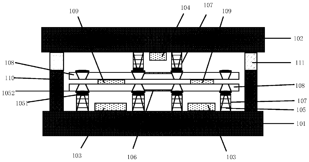
[0040] The invention provides a wafer-level heterogeneous integrated high-frequency system, the structure is as follows figure 1 As shown, it includes at least a first substrate 101, a second substrate 102, an insulating bonding layer, and at least two chips arranged in different layers; wherein:

[0041] The second substrate 102, the insulating bonding layer, and at least two chips are disposed between the first substrate 101 and the second substrate 102, including a first chip 103 connected to the first substrate 101, and a first chip 103 connected to the first substrate 101. the second chip 104 connected to the second substrate 102;

[0042] At least one through hole 105 is provided on the insulating bonding layer, and the side wall of the through hole 105 is coated with a conductive coating; ...


PUM


Abstract

The invention relates to a wafer level hetero integrated high frequency system and a production method thereof. The system at least comprises a first substrate, a second substrate, an insulated bonding layer and at least two chips. The second substrate, the insulated bonding layer and the at least two chips are set between the first substrate and the second substrate. The at least two chips comprise a first chip connected with the first substrate and a second chip connected with the second substrate. At least one through hole is set on the insulated bonding layer. A conductive coating is coated on the side wall of the through hole. One of the at least two chips is connected with the first substrate. The other in the at least two chips is connected with the second substrate. The at least two chips are electrically connected through the through hole. Inter-wafer bonding layer alignment materials are set on the first substrate and / or the second substrate. The inter-wafer bonding layer alignment materials are in support connection with the first substrate and the second substrate. According to the embodiment of the invention, the system integration degree is effectively improved, and aminiaturization target is realized.

Description

technical field [0001] The invention belongs to the technical field of microelectronics, and in particular relates to a wafer-level heterogeneous integrated high-frequency system and a manufacturing method thereof. Background technique [0002] With the continuous development of semiconductor chip manufacturing technology and electronic systems, the requirements of miniaturization, multi-function, high-frequency and high-speed operation, and low cost have gradually evolved into future communication systems, space and military system applications, high-definition cameras and sensors, and automotive radar. such as the focus of the application. [0003] Compound semiconductor materials have their unique advantages, so that semiconductor devices made of compounds also have their unique properties. In order to further improve the overall performance of the system, people specifically select the best substrate for fabricating the device according to the function of the required d...

Claims


Application Information

Patent Timeline
Patent Type & Authority Patents(China)
IPC IPC(8): H01L23/48H01L23/52H01L21/60B81C1/00
CPCB81C1/00H01L23/48H01L23/52H01L24/11
Inventor 马晓华郝跃易楚朋祝杰杰赵子越
Owner XIDIAN UNIV
Why Eureka
Try Eureka