Stress-regulated ultraviolet multi-wavelength MSM photoelectric detector and preparation method thereof

A photodetector and stress control technology, applied in circuits, electrical components, semiconductor devices, etc., can solve the problems of increasing device volume and increasing difficulty in precise splicing of sub-modules, achieving small device size, high integration, and The effect of simplifying the material structure

Pending Publication Date: 2018-08-21
XIAMEN UNIV
View PDF2 Cites 1 Cited by
  • Summary
  • Abstract
  • Description
  • Claims
  • Application Information

AI Technical Summary

Problems solved by technology

However, this multi-band system is equivalent to the integration of multiple sub-modules. With the increase of the detected wav

Method used


Image

  • Stress-regulated ultraviolet multi-wavelength MSM photoelectric detector and preparation method thereof
  • Stress-regulated ultraviolet multi-wavelength MSM photoelectric detector and preparation method thereof
  • Stress-regulated ultraviolet multi-wavelength MSM photoelectric detector and preparation method thereof

Examples


Embodiment 1

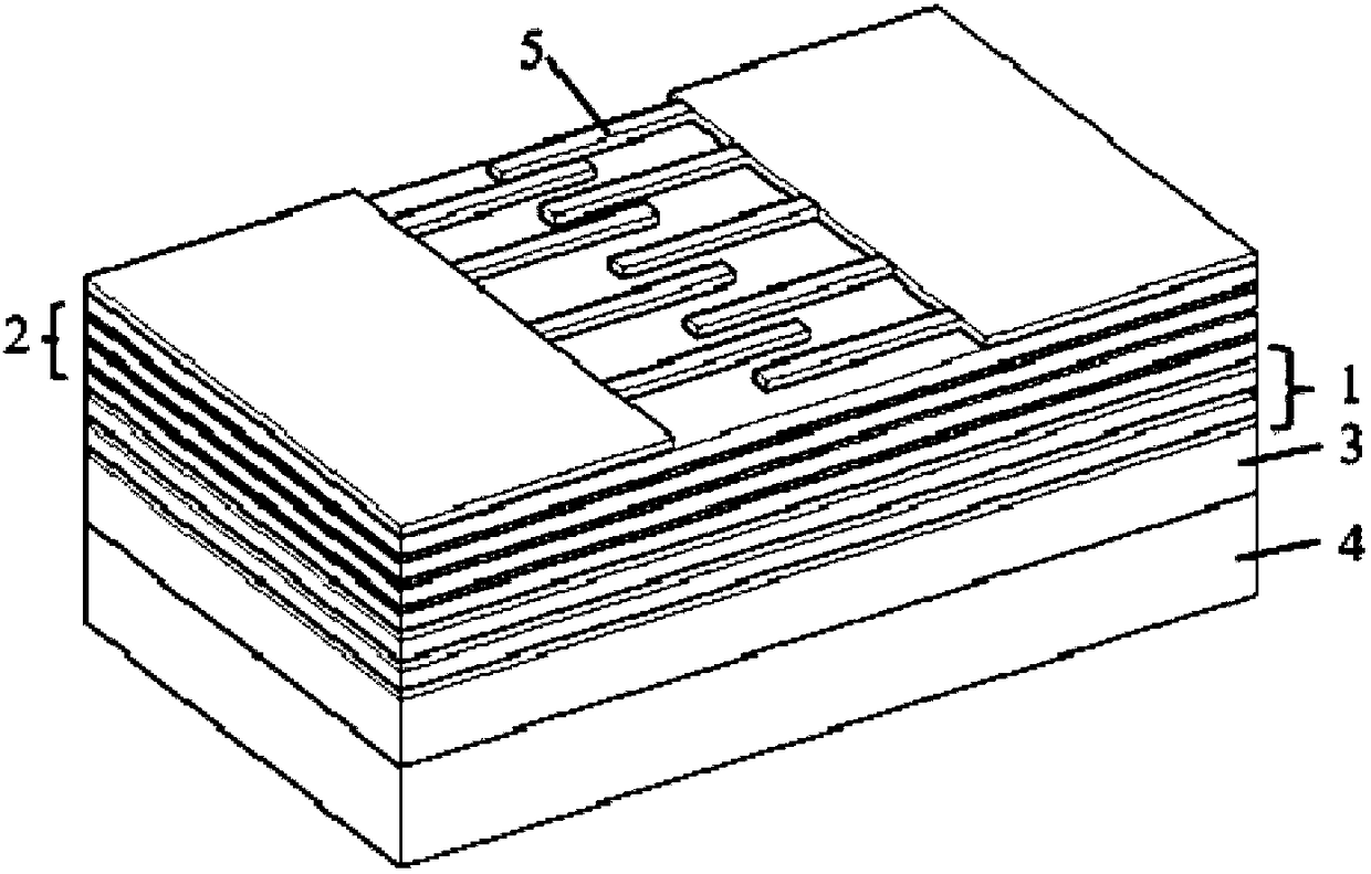
[0060] The preparation method of the stress-regulated ultraviolet multi-wavelength MSM photodetector of the overall planar MSM metal interdigitated electrode 5, the steps are as follows:

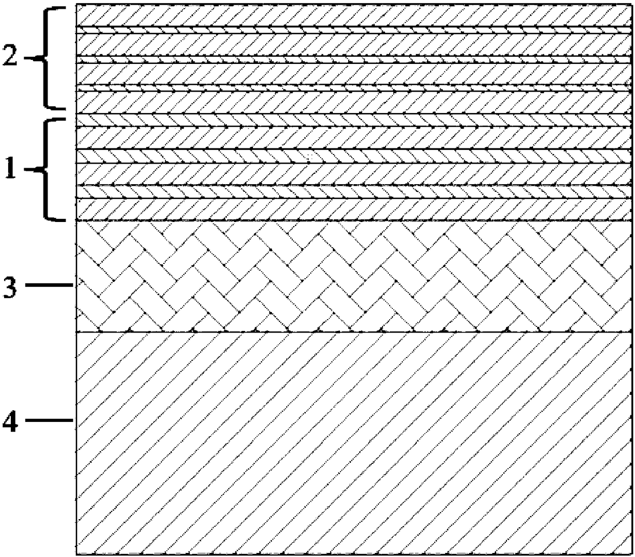
[0061] 1) Growth buffer layer 3. Ultrashort period superlattice strained layer, specifically:

[0062] 1.1) Using metal-organic vapor phase epitaxy technology, at a high temperature of 1100°C and a reaction chamber pressure of 100Torr, use H 2 Purge the sapphire substrate 4 to remove surface contamination; pre-pass TMA to form an Al-rich surface; then cool down to 570°C and use high-purity H 2 As carrier gas, NH 3 Pass into the reaction chamber to carry out substrate 4 nitriding;

[0063] 1.2) Raise the temperature to 800°C and feed TMA and NH 3 grow an AlN low-temperature buffer layer 3 with a thickness of about 20 nm, and then increase the temperature to 1090° C., and grow an AlN buffer layer 3 with a thickness of about 1 μm on the surface of the sapphire substrate 4 at a low pressure o...

Embodiment 2

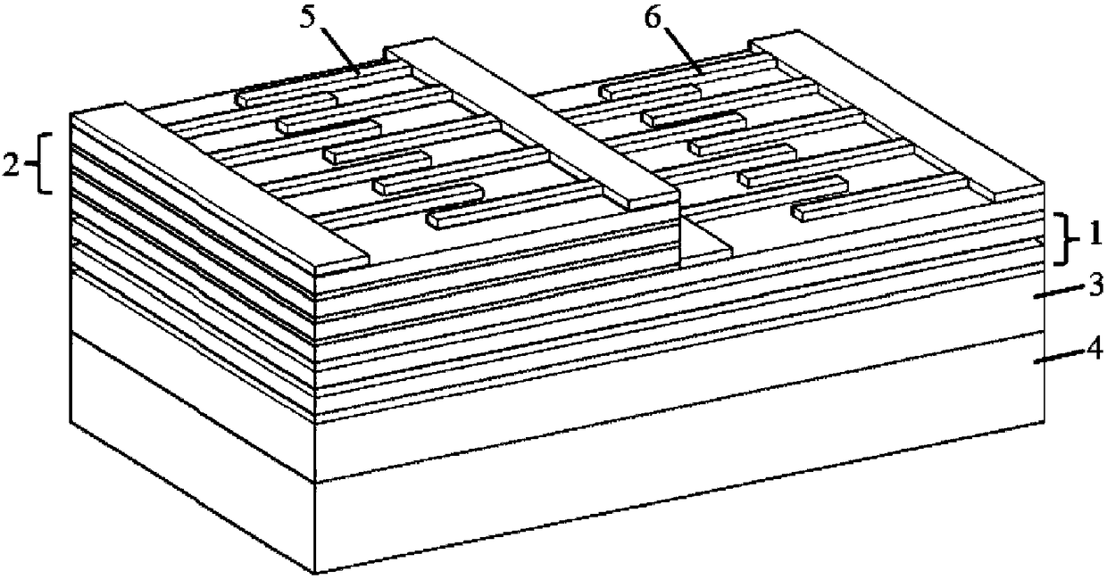
[0072] The preparation method of the stress-regulated ultraviolet multi-wavelength MSM photodetector of two sets of independent planar MSM metal interdigitated electrodes 5 is as follows:

[0073] Step 1) The material structure is basically the same as that of Example 1, the main difference is that when the metal interdigitated electrodes 5 are independently arranged on the first ultrashort period superlattice strained layer 1 and the second ultrashort period superlattice strained layer 2 For the upper surface, in step 1.3), the growth period of the second ultrashort period superlattice strained layer 2 is 20 to 200;

[0074] 2) Prepare two sets of independent planar MSM metal interdigitated electrodes 5, specifically:

[0075] 2.1) Use the same chemical cleaning steps as in Example 1 to completely remove the contamination and oxide layer on the surface of the epitaxial material;

[0076] 2.2) Use inductively coupled plasma (ICP) technology to etch the mesa, cover part of the...


PUM


Abstract

The invention relates to a stress-regulated ultraviolet multi-wavelength MSM photoelectric detector and a preparation method thereof. According to the photoelectric detector, ultraviolet double-wavelength narrow-linewidth detection is completed by using two sets of complete strain ultra-short period superlattice structures externally extending to a same substrate, the material structure, growth process and preparation technology of a double-wavelength detector are greatly simplified, and through precise selection and high integration, the basis is provided for multi-wavelength integrated colorimaging. According to the photoelectric detector, by regulating and controlling the layer number of trap molecules and base molecules of a single-period superlattice, the trap molecules and the basemolecules reach a force balance state nearby a coherent interface and are in complete strain; by designing and forming two sets of complete strain ultra-short period superlattices, double-wavelength detection on ultraviolet light signals can be achieved. According to the photoelectric detector, through multiple sets of ultra-short period superlattices which are generated on the epitaxial substratein the same crystal orientation and have different trap-base ratios, multiple band gaps are located in a preset wavelength range, more narrow-linewidth wavelength ultraviolet detection can be obtained, and accordingly the premise is provided for multi-wavelength integrated color imaging detection.

Description

technical field [0001] The invention relates to the technical field of semiconductor optoelectronic devices, more specifically, to a stress-regulated ultraviolet multi-wavelength MSM photodetector and a preparation method of the stress-regulated ultraviolet multi-wavelength MSM photodetector. Background technique [0002] As a dual-use detection technology for both military and civilian purposes, ultraviolet detection technology has a wide range of application requirements in the fields of missile guidance and early warning, aerospace tracking and control, ultraviolet non-line-of-sight optical communication, and biochemical medical detection and analysis. In recent years, with the continuous improvement of the quality of ultraviolet detection materials and device performance, people are looking forward to ultraviolet photodetectors with better performance and stronger functions to obtain richer target information. Therefore, the functions of the existing single-band ultravio...

Claims


Application Information

Patent Timeline
IPC IPC(8): H01L31/102H01L31/18
CPCH01L31/102H01L31/18Y02P70/50
Inventor 高娜冯向卢诗强黄凯陈航洋李书平康俊勇
Owner XIAMEN UNIV
Why Eureka
Try Eureka