Thin film field effect transistor type gas sensor and preparation method thereof

A thin-film field effect and gas sensor technology, which is applied in the direction of transistor, semiconductor/solid-state device manufacturing, semiconductor devices, etc., can solve the problems of unsuitable air atmosphere, limit low-power gas sensing, etc., and achieve improved sensitivity, room temperature gas sensitivity Enhanced effects and wide application scenarios

Active Publication Date: 2018-08-24
HUAZHONG UNIV OF SCI & TECH +1
View PDF9 Cites 26 Cited by
  • Summary
  • Abstract
  • Description
  • Claims
  • Application Information

AI Technical Summary

Problems solved by technology

In 2012, the Institute of Nanotechnology of the Karlsruhe Institute of Technology in Germany reported for the first time about the thin film field effect transistor of tin oxide, and the mobility of the device prepared by a simple spin-coating process can reach 0.13cm 2 V -1 the s -1 , the switching ratio is 85, and the threshold voltage is -1.9V, but at the same time, it also needs a higher gate voltage (above -50V) and source-drain voltage (-90V) and a harsh experimental environment (testing in an inert atmosphere) to fully realize High mobility; the harsh conditions required for high mobility also objectively limit the development of low-power gas sensing in practical applications, so this existing technology has not been used to detect gases
However, this high-mobility, all-quantum-dot FET needs to be inert (N 2 ) atmosphere preparation and testing can be realized, not suitable for use in real air atmosphere
[0008] In summary, the existing technologies can be summarized into two categories: 1) use quantum dots combined with traditional ceramic substrates to obtain a two-terminal device structure as a gas sensor; 2) use quantum dots combined with micro-nano technology to prepare three-terminal FET devices, and inert The electrical properties of semiconductors are tested in the environment, and it can be seen that quantum dot FETs are not used as gas sensors in the prior art (because the thin film field effect transistor TFT is a kind of field effect transistor FET, of course there is no quantum dot thin film in the prior art Field-effect transistor TFT is used for gas sensing), and there is no precedent at home and abroad to use quantum dot materials to prepare thin-film field-effect transistors and apply them to gas sensing in actual air atmospheres.

Method used


Image

  • Thin film field effect transistor type gas sensor and preparation method thereof
  • Thin film field effect transistor type gas sensor and preparation method thereof
  • Thin film field effect transistor type gas sensor and preparation method thereof

Examples


Embodiment 1

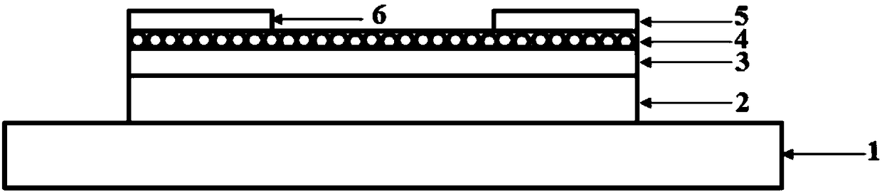
[0052] Embodiment 1: prepare bottom gate top contact type PbS quantum dot thin film field effect transistor type gas sensor (such as figure 1 shown), specifically may include the following steps:

[0053] (1) Preparation of PbS colloidal quantum dot solution. PbO can be used as the lead source, and hexamethyldisilathane (TMS) can be used as the sulfur source, which can be produced by colloid chemical reaction.

[0054] Specifically, 0.9 g of PbO can be dissolved in 5 ml of oleic acid (OA) and 20 ml of octadecene (ODE) under a nitrogen atmosphere and heated to 90° C. to prepare a precursor of lead oleate as a lead source. After evacuating for 8 hours, the temperature of the precursor was raised to 120°C. Dissolve 280 μl TMS into 10 ml ODE as a sulfur source. Rapidly inject the sulfur source into the lead source at 120°C, and after the color of the reaction system turns black (about 15s), put the solution into cold water to rapidly drop the temperature to room temperature. A...

Embodiment 2

[0063] Example 2: Preparation of bottom-gate top-contact SnO 2 Quantum dot thin film field effect transistor type gas sensor (such as figure 1 shown), specifically may include the following steps:

[0064] (1) Preparation of SnO 2 Colloidal quantum dot solution. SnCl can be used 4 ·5H 2 O is used as a tin source, and oleic acid and oleylamine long-chain organic ligands are used as encapsulating agents, which are produced by colloidal chemical reaction.

[0065] Specifically, 0.6g SnCl can be 4 ·5H 2 O. 20ml of oleic acid and 2.5ml of oleylamine were heated to 100°C and vacuum-dried until the reaction was clear, cooled to 60°C, 10ml of ethanol was taken out and mixed evenly, then added to a stainless steel autoclave, and placed in an oven at 180°C for 3 hours. After the reaction is completed, take it out, and when it is cooled to room temperature, take out the solution in the autoclave, mix it with ethanol and centrifuge the precipitate, then disperse the precipitated pr...

Embodiment 3

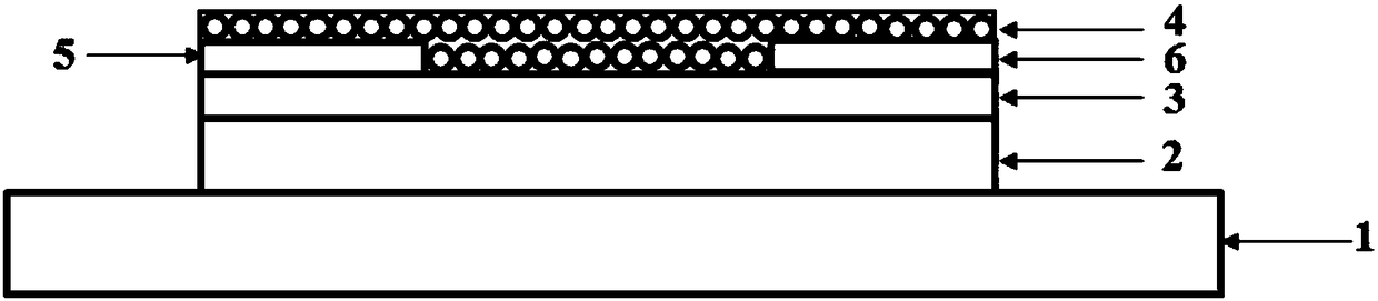
[0067] Embodiment 3: prepare bottom gate bottom contact type PbS quantum dot thin film field effect transistor type gas sensor (such as figure 2 shown), specifically include the following steps:

[0068] (1) Preparation of PbS colloidal quantum dot solution. PbO can be used as the lead source, and hexamethyldisilathane (TMS) can be used as the sulfur source, which can be produced by colloid chemical reaction.

[0069] Specifically, 0.9 g of PbO can be dissolved in 5 ml of oleic acid (OA) and 20 ml of octadecene (ODE) under a nitrogen atmosphere and heated to 90° C. to prepare a precursor of lead oleate as a lead source. After evacuating for 8 hours, the temperature of the precursor was raised to 120°C. Dissolve 280 μl TMS into 10 ml ODE as a sulfur source. Rapidly inject the sulfur source into the lead source at 120°C, and after the color of the reaction system turns black (about 15s), put the solution into cold water to rapidly drop the temperature to room temperature. A...


PUM

PropertyMeasurementUnit
thicknessaaaaaaaaaa
concentrationaaaaaaaaaa

Abstract

The invention discloses a thin film field effect transistor type gas sensor and a preparation method thereof. The sensor is a thin film field effect transistor with a bottom gate top contact type structure or a bottom gate bottom contact type structure. A thin film field effect transistor with a bottom grid top contact structure is taken as an example. The transistor comprises a substrate, a gateinsulating layer and a channel active layer from bottom to top. The channel active layer is a quantum dot thin film. A source electrode and a drain electrode are deposited above the substrate. A gateelectrode is further led out of the substrate. The internal composition, the structure, the overall process of the corresponding preparation method and the parameters during all steps of the preparation method of the thin film field effect transistor type gas sensor are improved. The quantum dot thin film serves as a channel active layer and a gas sensitive layer at the same time, and the gas response of multiple parameters is comprehensively regulated by utilizing the grid bias voltage. As a result, the prepared gas sensor is high in sensitivity, low in power consumption and high in selectivity. The effect of detecting low-concentration target gases, such as NO2 and H2S, is achieved.

Description

technical field [0001] The invention belongs to the technical field of gas sensors, and more specifically relates to a thin film field effect transistor type gas sensor and a preparation method thereof. layer thin film field effect transistor type (gas sensor. Background technique [0002] Traditional semiconductor gas sensors are usually based on layers of gas-sensitive materials (such as SnO 2 , ZnO, TiO 2 etc.) when in contact with gas, the resistance value changes to achieve the effect of gas detection. It has the characteristics of simple measurement method, high sensitivity, fast response, convenient operation, good portability, and low cost. However, this type of gas sensor generally adopts mature technology but Relatively large tubular or chip ceramic substrates, and commercial sensors must work at higher operating temperatures (200-600°C), resulting in higher power consumption, which reduces the portability and integration of sensors. Moreover, it also increases ...

Claims


Application Information

Patent Timeline
Patent Type & Authority Applications(China)
IPC IPC(8): H01L29/786H01L29/22H01L29/24H01L29/06H01L21/34G01N27/414
CPCG01N27/4141G01N27/4146H01L29/0665H01L29/22H01L29/24H01L29/66969H01L29/786H01L29/7869
Inventor 刘欢唐江张建兵刘竞尧胡志响易飞张光祖
Owner HUAZHONG UNIV OF SCI & TECH
Why Eureka
Try Eureka