A coil, a dielectric cylinder and a plasma chamber

A plasma and chamber technology, applied in the field of plasma chambers, can solve problems such as insufficient plasma density, wafer surface damage, and slow etching rate

Active Publication Date: 2021-04-09
BEIJING NAURA MICROELECTRONICS EQUIP CO LTD
View PDF15 Cites 0 Cited by
  • Summary
  • Abstract
  • Description
  • Claims
  • Application Information

AI Technical Summary

Problems solved by technology

[0007] But the magnetic field produced by the first solenoid 18 in the prior art two is as image 3 As shown, the magnetic field is inhomogeneous in the section along the axial direction of the first solenoid 18, and the magnetic field in the center of the chamber is relatively weak, and the direction of the magnetic field is along the axial direction of the first solenoid 18 and perpendicular to the first solenoid 18. There is almost no magnetic field in the horizontal direction of the axial direction of a solenoid 18; this causes insufficient electronic confinement in the horizontal direction perpendicular to the axial direction of the first solenoid 18 in the first solenoid 18, so that the excitation area of ​​the planar inductive coil is separated Under the constraint of an external magnetic field, the cyclotron collision of electrons is not sufficient, and the electron energy is still high, which is easy to cause damage to the wafer surface; at the same time, the plasma density is not high enough, and the etching rate is still slow

Method used


Image

  • A coil, a dielectric cylinder and a plasma chamber
  • A coil, a dielectric cylinder and a plasma chamber
  • A coil, a dielectric cylinder and a plasma chamber

Examples


Embodiment 1

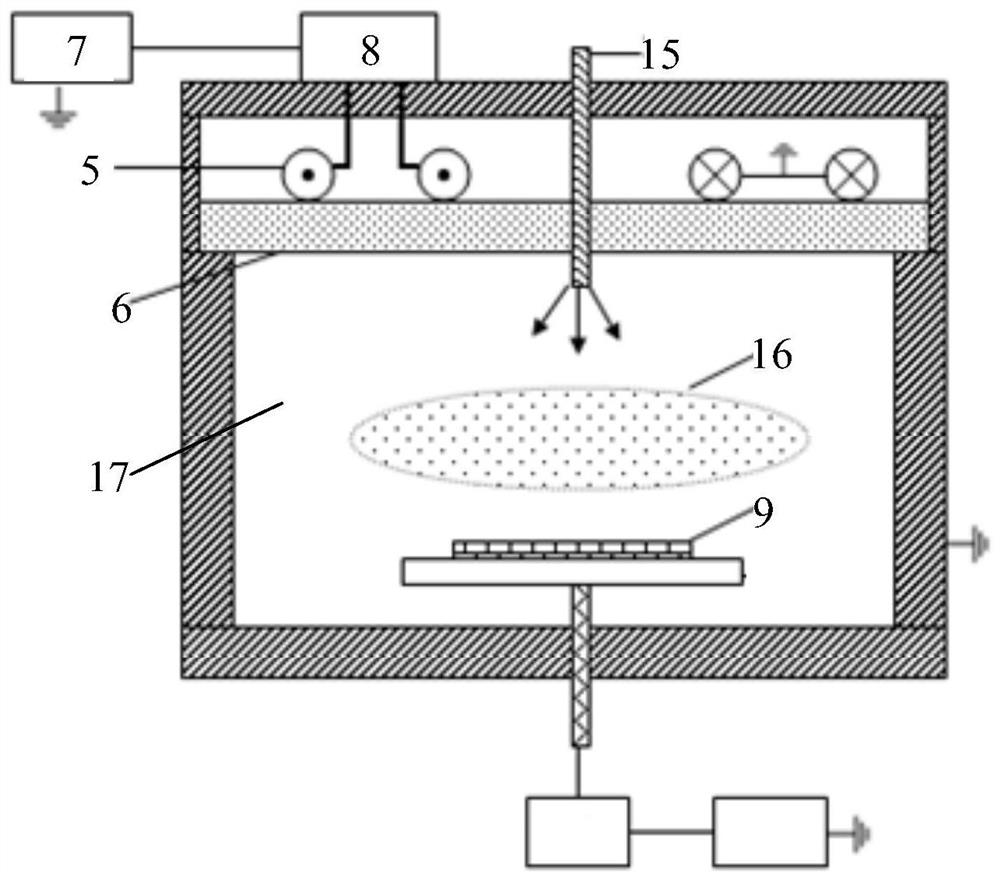
[0047] This embodiment provides a coil, such as Figure 4-Figure 7 As shown, including a solenoid 1 and a sub-coil 2 arranged on the solenoid 1, the angle between the axis of the sub-coil 2 and the axis of the solenoid 1 is greater than 0° and less than 180°, so that the magnetic field generated by the sub-coil 2 The magnetic field generated by the solenoid 1 has a different direction to increase the horizontal component of the magnetic field lines inside the solenoid 1 .

[0048] The coil is provided with a sub-coil 2 on the solenoid 1, and the angle between the axis of the sub-coil 2 and the axis of the solenoid 1 is greater than 0° and less than 180°, when the current is passed into the solenoid 1 and the sub-coil 2 , a magnetic field along its axial direction can be generated in the solenoid 1, and a magnetic field along its axial direction can be generated in the sub-coil 2 at the same time, the magnetic field generated in the solenoid 1 and the magnetic field generated i...

Embodiment 2

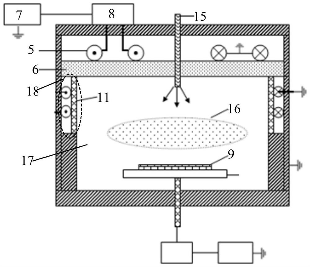
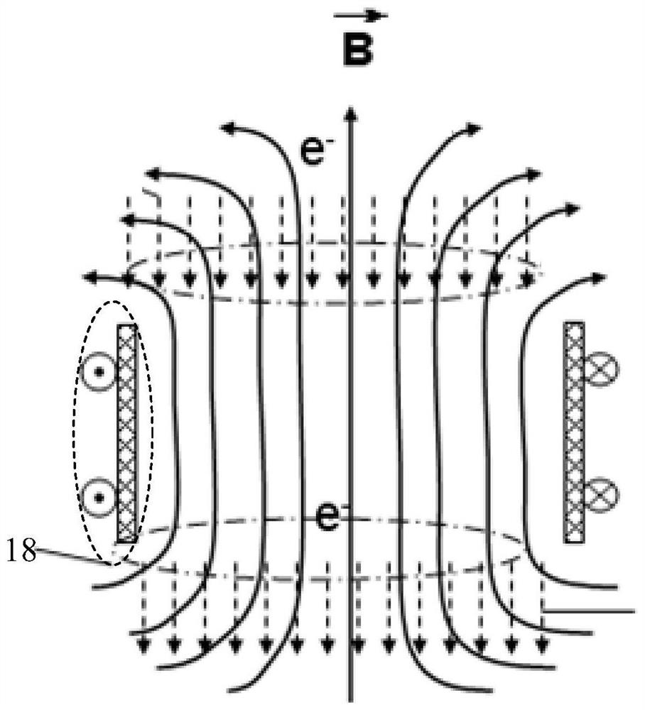
[0058] A coil is provided in this embodiment, and the difference from Embodiment 1 is, as Figure 8 As shown, the winding shape of the sub-coil 2 is semi-circular, and the sub-coil 2 of the same circle is located on the same side of its corresponding sub-core 3; the sub-coil 2 of two adjacent turns is located on different sides of its corresponding sub-core 3 . Correspondingly, the current directions in the two adjacent turns of the coil 2 are opposite.

[0059] Wherein, taking the sub-coil 2 wound on the solenoid 1 as two turns as an example, as Figure 9 As shown, the sub-coil 2 is first wound around the solenoid 1 once, and the coil 2 is located on the upper side of a coil core 3. After the coil 2 is wound, the wire of the coil 2 crosses to the phase The adjacent next circle of magnetic core 3, and wound to the lower side of the next circle of magnetic core 3. After the winding is completed, a current is passed into the wire, and the flow direction of the current in the ...

Embodiment 3

[0064] This embodiment provides a coil, which is different from Embodiment 1-2, such as Figure 10 As shown, the winding shape of the sub-coil 2 is circular, and the sub-coil 2 corresponds to winding the sub-magnetic core 3 once, and the current direction in two adjacent turns of the sub-coil 2 is the same.

[0065] Such setting can make the magnetic field formed by the sub-coil 2 in the position corresponding to the sub-magnetic core 3 in the solenoid 1 have a larger range, so that when the number of sub-magnetic cores 3 on the solenoid 1 and the number of distributed turns are the same, the sub-coil 2 The range of the magnetic field area where the magnetic field is generated in the solenoid 1 is correspondingly increased, thereby increasing the probability of the plasma whirling and colliding in the solenoid 1, and then effectively reducing the energy and temperature of the electrons in the plasma, and finally The damage to the wafer surface after the electrons bombard the w...


PUM


Abstract

The present invention provides a coil, a dielectric cartridge and a plasma chamber. The coil includes a solenoid and a sub-coil arranged on the solenoid; the included angle between the axis of the sub-coil and the axis of the solenoid is greater than 0° and less than 180°, so that the magnetic field generated by the sub-coil and the magnetic field generated by the solenoid Have different directions to increase the horizontal component of the magnetic field lines inside the solenoid. The plasma chamber of the present invention includes a cavity body and a main plasma generating device; the main plasma generating device comprises: a radio frequency power supply, a matching device and a main coil, and the radio frequency power supply is electrically connected with the main coil through the matching device to generate plasma; the plasma chamber The chamber also includes an auxiliary plasma generating device arranged on the side wall of the cavity; the auxiliary plasma generating device includes an excitation power source and a coil of the present invention; the coil is sleeved on the inner side of the side wall of the cavity. Using the plasma chamber of the coil of the invention, the horizontal component of the magnetic force line in the chamber is increased, the surface damage of the wafer is reduced, and the processing rate thereof is improved.

Description

technical field [0001] The invention relates to the technical field of plasma processing, in particular to a coil, a dielectric cylinder and a plasma chamber. Background technique [0002] With the development of semiconductor process technology, various semiconductor devices are widely used in semiconductor process. Plasma etching or deposition is a key step in the semiconductor manufacturing process. The working principle of plasma etching or deposition is to process gases (such as argon Ar, helium He, nitrogen N 2 , hydrogen H 2 , Chlorine Cl 2 , boron trichloride BCl 3 , Octafluorocyclobutane C 4 f 8 , Tetrafluoromethane CF 4 , sulfur hexafluoride SF 6 etc.) into the vacuum chamber, the process gas is dissociated, excited, ionized, etc. by means of electrical excitation or optical excitation. Interaction, corresponding etching and deposition. [0003] Complex semiconductor processes are often accompanied by etching and deposition of different semiconductor mater...

Claims


Application Information

Patent Timeline
Patent Type & Authority Patents(China)
IPC IPC(8): H05H1/46H01L21/67
CPCH01L21/67005H01L2221/67H05H1/46
Inventor 肖德志琚里
Owner BEIJING NAURA MICROELECTRONICS EQUIP CO LTD
Why Eureka
Try Eureka