

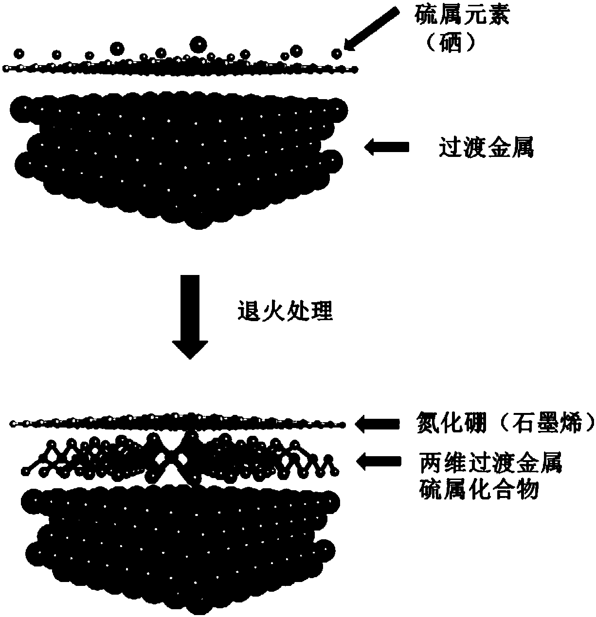
Preparation method of transition metal chalcogenides and boron nitride or graphene heterojunction
A technology of chalcogen compounds and transition metals, applied in the field of nanomaterials, can solve the problem of lack of band gap in electronic structure, and achieve the effect of easy structure control and simple method
- Summary
- Abstract
- Description
- Claims
- Application Information
AI Technical Summary
Problems solved by technology
Method used
Image


Examples
Embodiment 1
[0043] Preparation of ruthenium selenide-boron nitride heterojunction.
[0044] 1) Processing Ru(0001) single crystal
[0045] Argon ion sputtering (2kV, 1×10 -5 mbar Ar, 10min), oxygen burning (527 degrees, 1.6×10 -6 mbar O 2, 10min), and then heated the Ru single crystal and kept it at a high temperature of 1200 degrees for 10 minutes for annealing, until no impurities were observed by X-ray photoelectron spectroscopy and scanning tunneling microscope.
[0046] 2) Growth of boron nitride on Ru(0001) surface
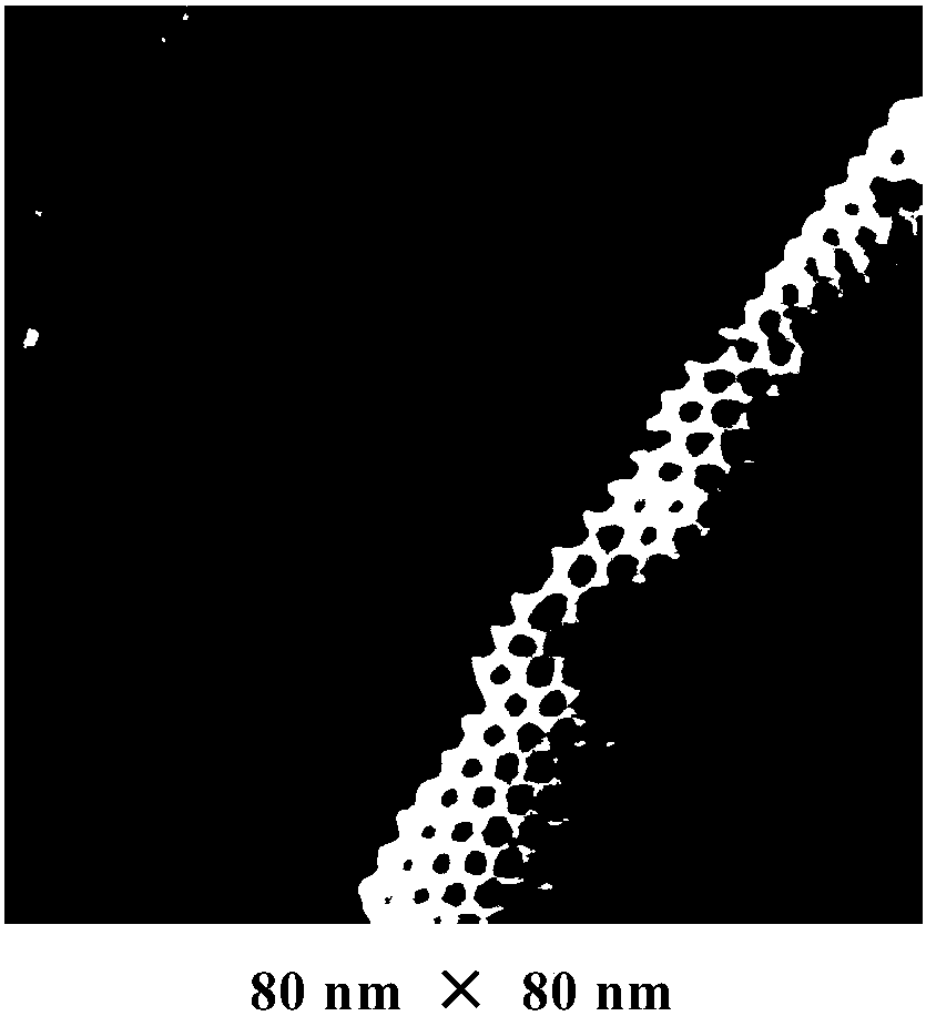
[0047] Boron nitride is grown on the Ru(0001) substrate by chemical vapor deposition, the boron source used is borazine, which is liquid at room temperature, and the air in the borazine is removed by liquid nitrogen before use . Then the cleaned Ru(0001) substrate was heated to 750°C and passed through 5.2×10 -8 mbar's borazine, borazine dissociates and splices on the substrate to obtain boron nitride. By adjusting the passage time of borazine, the coverage of bor...
Embodiment 2
[0051] Preparation of platinum selenide-boron nitride heterojunction.
[0052] 1) Processing Pt(111) single crystal
[0053] Argon ion sputtering (2kV, 1×10 -5 mbar Ar, 10min), oxygen burning (527 degrees, 1.6×10 -6 mbar O 2 ,10min), and then heated the Pt single crystal and maintained it at a high temperature of 850°C for 10 minutes for annealing, until no impurities were observed by X-ray photoelectron spectroscopy and scanning tunneling microscope.
[0054] 2) Growth of boron nitride on the surface of Pt(111)
[0055] Boron nitride is grown on a Pt(111) substrate by chemical vapor deposition. The boron source used is borazine. Borazine is liquid at room temperature. Before use, liquid nitrogen is used to remove the air in borazine. . Then the cleaned Pt(111) substrate was heated to 760 degrees and passed through 5.2×10 -7 mbar's borazine, borazine dissociates and splices on the substrate to obtain boron nitride. By adjusting the passage time of borazine, the coverage ...
PUM
 Abstract
Description
Claims
Application Information