


Quick Research
Generate reliable direction feasibility study reports for your R&D in just a few steps.

Technical Q&A
Discover and master advanced knowledge NOW. Basics, ideas, possibilities, all at once.

Find Solutions
As an expert in R&D theories, this can generate solutions to your technical problems instantly.

Evaluate Feasibility
Analyze your overall solution with one click, know your potential R&D risks in advance.

Monitor Landscape
Get weekly tech updates, stay abreast of the latest tech innovations and key insights.
Flexible nanoimprint template and preparation method thereof
A technology of nanoimprinting and template, which is applied in the direction of photomechanical equipment, patterned surface photolithography, optics, etc. It can solve the problems of further improvement of mechanical properties, high cost of silicon template preparation, and inability to make flexible templates. Achieve good light acid corrosion resistance, good mechanical properties, and good thermal conductivity
- Summary
- Abstract
- Description
- Claims
- Application Information
AI Technical Summary
Problems solved by technology
Method used
Image


Examples
Embodiment 1
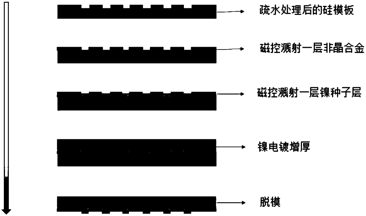
[0060] Put 10 microliters of FDTS (1H,1H,2H,2H-perfluorodecyltrichlorosilane) into 20ml of heptane, and then soak the prepared silicon template for 10 minutes, then remove the silicon template with pure Wash with heptane, and finally bake on a hot plate at 100°C for 10 minutes to complete the hydrophobic treatment of the silicon template. The next step is magnetron sputtering, with Zr 55 Cu 30 Ni 5 al 10 A single target of composition sputters a 1 micron thick amorphous alloy film on a silicon template with a power of 70W. Then sputter a layer of about 100nm nickel as a seed layer, and then perform electroplating in a nickel sulfamate solution to thicken it to about 100 microns. Finally, the amorphous alloy layer and the nickel base layer are peeled off from the silicon template to make a flexible nanoimprint template. The manufacturing process of the flexible nanoimprint template in this embodiment is as follows figure 2 shown.
[0061] Fig. 5(a) is a SEM image of the ...
Embodiment 2
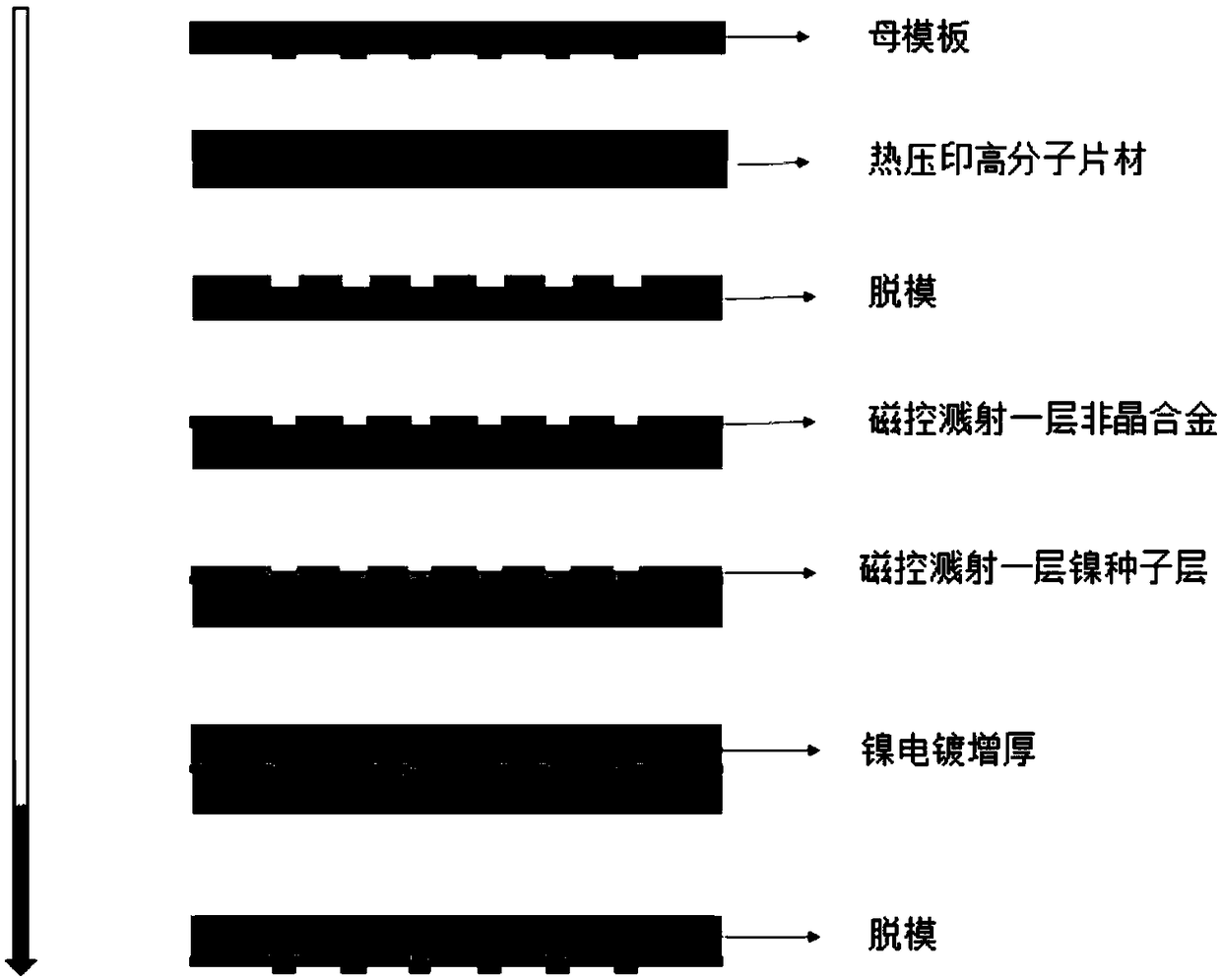
[0063] The fabricated silicon template with a 600nm line width grating was thermally embossed on a polycarbonate sheet (PC) at 175° C. with a pressure of 500 MPa. Subsequent next step is magnetron sputtering, with Zr 55 Cu 30 Ni 5 al 10 A single target of composition sputters an amorphous alloy film about 1 micron thick on a silicon template with a power of 70W. Then sputter a layer of about 100nm nickel as a seed layer, and then perform electroplating in a nickel sulfamate solution to thicken it to about 100 microns. Finally, the amorphous alloy layer and the nickel base layer are peeled off from the PC sheet to make a flexible nanoimprint template. The manufacturing process of the flexible nanoimprint template in this embodiment is as follows image 3 shown.
[0064] Fig. 6(a) is a SEM image of the flexible nanoimprint template prepared in this example, and Fig. 6(b) is an AFM image of the flexible nanoimprint template prepared in this example. It can be seen from Figu...
Embodiment 3
[0066] Spin-coat a layer of electron beam photoresist HSQ on a silicon wafer or ITO conductive glass, and then use an electron beam to write nanoscale patterns on the HSQ on a silicon wafer or ITO glass, and then perform magnetron sputtering after development, using Zr 55 Cu 30 Ni 5 al 10 A single target of composition sputters a 1 micron thick amorphous alloy film on a silicon template with a power of 70W. Then sputter a layer of about 100nm nickel as a seed layer, and then perform electroplating in a nickel sulfamate solution to thicken it to about 100 microns. Finally, the amorphous alloy layer and the nickel base layer are peeled off from the silicon template or the ITO template to make a flexible nanoimprint template. The manufacturing process of the flexible nanoimprint template in this embodiment is as follows Figure 4 shown.
[0067] The flexible nano-imprint template prepared in Examples 1-3 was tested by a nano-indentation instrument, and the Young's modulus was...
PUM
| Property | Measurement | Unit |
|---|---|---|
| Thickness | aaaaa | aaaaa |
| Thickness | aaaaa | aaaaa |
| Thickness | aaaaa | aaaaa |
Abstract
Description
Claims
Application Information
 - R&D Engineer
- R&D Manager
- IP Professional
- Industry Leading Data Capabilities
- Powerful AI technology
- Patent DNA Extraction
Browse by: Latest US Patents, China's latest patents, Technical Efficacy Thesaurus, Application Domain, Technology Topic, Popular Technical Reports.
© 2024 PatSnap. All rights reserved.Legal|Privacy policy|Modern Slavery Act Transparency Statement|Sitemap|About US| Contact US: help@patsnap.com