A method for preparing metal oxide thin film transistors at low temperature
A technology of oxide thin films and transistors, which is applied in semiconductor devices, semiconductor/solid-state device manufacturing, electrical components, etc., can solve the problems of high process temperature of polysilicon thin film transistors, poor uniformity of transistor performance, and low field effect mobility. Low, good product performance, and the effect of environmental protection
- Summary
- Abstract
- Description
- Claims
- Application Information
AI Technical Summary
Problems solved by technology
Method used
Image

Examples
preparation example Construction
[0043] Such as Figure 1-Figure 7 As shown, the present invention provides a method for preparing a metal oxide thin film transistor at a low temperature. The present invention is a method for preparing a metal oxide thin film transistor at a low temperature based on a solution method. On the premise of ensuring the electrical performance of the transistor, the low temperature preparation of TFT is further realized. , thereby reducing the influence of the preparation process on the flexible substrate. The method comprises the steps of:
[0044] (1), In 2 o 3 Preparation of the precursor solution of the base or ZnO-based oxide: Here, In 2 o 3 The preparation of the precursor solution is taken as an example. Dissolve indium nitrate in an aqueous solvent such as deionized water or ammonia water, and stir magnetically at 0-100°C for 0.5-24 hours to obtain a clear and transparent In 2 o 3 Precursor, where In 2 o 3 The concentration of the precursor solution is 0.01-0.5mol / L...
Embodiment 1
[0060] The substrate in this embodiment is a p-doped thermally oxidized silicon wafer purchased commercially and polished on one side, and the thickness of the thermally oxidized silicon is 100 nm. Indium nitrate powder was purchased from Alfa Company. Concrete preparation process is as follows:
[0061] Step 1: Preparation of In 2 o 3 For the precursor solution, dissolve indium nitrate in deionized water according to 0.2mol / L, and stir at room temperature on a magnetic stirring table for 6 hours to obtain a colorless and transparent In 2 o 3 Precursor solution, let it stand for later use; filter the precursor solution with a 0.22 μL water filter before use to remove insoluble impurities;
[0062] Step 2: Substrate cleaning: Clean the thermally oxidized silicon wafer after cutting with deionized water, acetone, isopropanol, and deionized water in an ultrasonic cleaning machine for 10 minutes each, and blow dry with nitrogen;
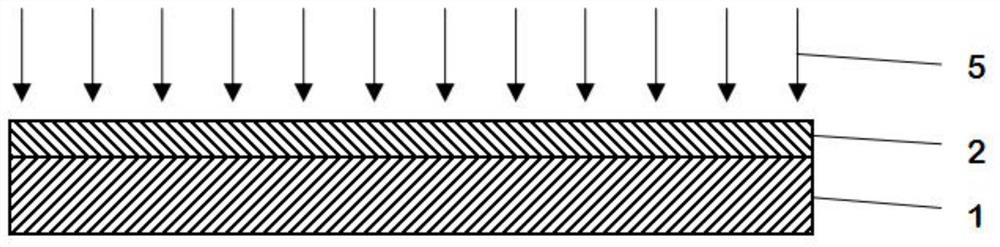
[0063] Step 3: If figure 1 As shown, the sur...
Embodiment 2
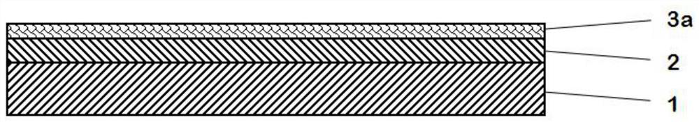
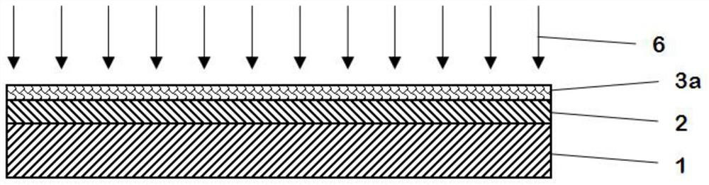
[0070] Relative to Example 1, after carrying out steps 1-4, discard the NH of step 5 3 For the plasma treatment process, proceed directly to steps 6-8. The effect of embodiment 2 is to serve as the comparison of embodiment 1, compare the pre-annealed In 2 o 3 film in the presence or absence of NH 3 The influence of plasma treatment process conditions on the electrical properties of its TFT, such as Figure 7 shown.
PUM
| Property | Measurement | Unit |
|---|---|---|
| thickness | aaaaa | aaaaa |
Abstract
Description
Claims
Application Information
 - R&D
- Intellectual Property
- Life Sciences
- Materials
- Tech Scout
- Unparalleled Data Quality
- Higher Quality Content
- 60% Fewer Hallucinations
Browse by: Latest US Patents, China's latest patents, Technical Efficacy Thesaurus, Application Domain, Technology Topic, Popular Technical Reports.
© 2025 PatSnap. All rights reserved.Legal|Privacy policy|Modern Slavery Act Transparency Statement|Sitemap|About US| Contact US: help@patsnap.com