A method for preparing a one-dimensional nanomaterial-based sensor

A technology of nanomaterials and sensors, which is applied in the field of preparation of one-dimensional nanomaterial sensors, can solve the problems of one-dimensional nanomaterial arrangement dependence, complex surface modification, complex process, etc., and achieve experimental cost saving, good combination, and arrangement good consistency

Inactive Publication Date: 2018-12-04
XI AN JIAOTONG UNIV
View PDF4 Cites 2 Cited by
  • Summary
  • Abstract
  • Description
  • Claims
  • Application Information

AI Technical Summary

Problems solved by technology

Fan et al. [Smith, P.A.; Nordquist, C.D.; Jackson, T.N.; Mayer, T.S.; Martin, B.R.; Mbindyo, J.; Mallouk, T.E. Electric-field assisted assembly and alignment of metallic nanowires. 77, 1399–1401.] Using contact printing to arrange semiconductor nanomaterials in an orderly manner, the surface may be damaged due to poor contact between the nanomaterials and the substrate
Whang et al [Whang, D.; Jin, S.; Wu, Y.; Lieber, C.M. Large-scale hierarchical organization of nanowire arrays for integrated nanosystems. Nano Lett. 2003, 3, 253–256.] used the Langmuir–Blodgett method to control a organization and hierarchy of one-dimensional silicon nanomaterials, however, this technique requires complex surface modification, and the arrangement of one-dimensional nanomaterials depends on the control of surface pressure
Zhang et al. [Zhang Q, Gupta S, Todd Emrick A, et al.Surface-Functionalized CdSe Nanorods for Assembly in Diblock Copolymer Templates[J].Journal of the American Chemical Society,2006,128(12):3898-3899.] CdSe nanorods were successfully assembled using geometric pattern template induction, but the process is relatively complicated
Most of the above methods require expensive instruments and equipment, and the cost is relatively high.

Method used


Image

  • A method for preparing a one-dimensional nanomaterial-based sensor
  • A method for preparing a one-dimensional nanomaterial-based sensor
  • A method for preparing a one-dimensional nanomaterial-based sensor

Examples


Embodiment 1

[0035] This example prepares a gas sensor based on the assembly method of zinc oxide nanowires to detect carbon monoxide, including the steps of preparing zinc oxide nanowires, the assembly steps of zinc oxide nanowires and the preparation steps of gas sensors, such as figure 1 It is a schematic diagram of the general flow of the invention;

[0036] The steps of preparing zinc oxide nanowires:

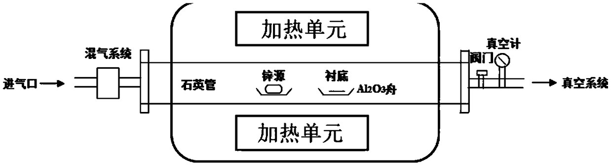
[0037] Preparation device such as figure 2As shown, the silicon wafer was cut into 2cm*2cm slices before preparation, and the silicon wafer was cleaned with ethanol, deionized water, and acetone for 5 minutes, and then placed on a hot plate to remove residual liquid. Zinc powder (purity 99.99%) was put into an alumina boat, the alumina boat was placed in the center of the quartz tube, and the substrate was placed 3-4 cm to the right of the zinc source. When the vacuum degree of the air passage is 10Pa with a mechanical pump, the temperature in the furnace is raised to 600-750°C, and...

Embodiment 2

[0058] In this embodiment, in order to verify the universality of the present invention, silicon nanowires are assembled, and the type of the substrate is changed at the same time, and a silicon substrate coated with a gold film is used.

[0059] Steps for preparing silicon nanowires:

[0060] (1) First, cut the p-type (100) direction single crystal silicon wafer into 1*1cm 2 Then immerse the silicon wafer in an ethanol solution, and perform ultrasonic cleaning in an ultrasonic cleaning tank for 10 minutes to remove surface organic matter;

[0061] (2) Put the silicon chip into the H of the configuration 2 SO 4: h 2 o 2 Ultrasonic cleaning in the solution for 10 minutes to further remove surface organic matter and form an oxide layer, and then clean the silicon wafer with 5% HF to remove the surface oxide layer;

[0062] (3) Configure different concentrations of HF-AgNO 3 Corrosion solution, placed in a 100ml reaction kettle with tetrafluoroethylene lining, the filling d...


PUM

PropertyMeasurementUnit
Sensitivityaaaaaaaaaa

Abstract

A method for preparing a one-dimensional nanomaterial-based sensor is disclosed. The method includes dropping a suspension of a one-dimensional nanomaterial onto a substrate; combing the suspension onthe substrate with a tool brush in a constant speed; then allowing the product to stand; drying the substrate so that the one-dimensional nanomaterial is more closely bonded with the substrate through the van der Waals force; after photoresist removing, allowing the solution on the surface of the substrate to volatize so that the one-dimensional nanomaterial is uniformly arranged on the substratein a large area; forming an interdigital electrode pattern through a photoetching process; and stripping after the substrate surface is plated with gold to obtain the one-dimensional nanomaterial-based sensor. The sensor has characteristics of excellent electrical properties and high sensitivity. The method is suitable for a plurality of one-dimensional nanomaterials such as zinc oxide and silicon, and is suitable for different substrates such as silica and glass. The distribution density and arrangement uniformity of the one-dimensional nanomaterial can be achieved through changing the dimension of an assembling tool, and large-area production is hoped to be possible if a large-dimension precise mechanical assembling tool is put into use. The method has a wide application prospect in thefield of manufacturing and integration of nanometer devices.

Description

technical field [0001] The invention belongs to the technical field of assembly of nanomaterials and preparation of sensors, in particular to a method for preparing a sensor based on one-dimensional nanomaterials. Background technique [0002] Sensor technology is one of the fast-growing high-tech technologies in today's world, and it is also an important symbol of the development of contemporary science and technology. The sensor research based on one-dimensional nanomaterials is the frontier hotspot of research in various countries, and it is an important part with the most application value in the field of sensor technology. As a versatile assembly unit, one-dimensional nanomaterials have attracted attention in many fields such as electronics, optics, bioscience, energy storage, etc. Compared with traditional planar semiconductor materials, one-dimensional nanomaterials have unique electrical and optical properties due to their larger specific surface area and two-dimens...

Claims


Application Information

Patent Timeline
Patent Type & Authority Applications(China)
IPC IPC(8): G01N27/12B82Y15/00
CPCB82Y15/00G01N27/127
Inventor 杨树明程碧瑶王一鸣杨晓凯王飞
Owner XI AN JIAOTONG UNIV
Why Eureka
Try Eureka