A process for preparing solar-grade N-type monocrystalline

A solar-grade, single-crystal silicon technology, applied in the field of preparation of solar-grade N-type single-crystal silicon, preparation of single-crystal silicon, and resistance control of N-type single-crystal silicon, which can solve the problem of disturbing the melt, unfavorable resistivity control, weakening Phosphorus-based N-type resistivity and other issues to achieve the effect of increasing concentration

Inactive Publication Date: 2018-12-18
包头美科硅能源有限公司
View PDF9 Cites 9 Cited by
  • Summary
  • Abstract
  • Description
  • Claims
  • Application Information

AI Technical Summary

Problems solved by technology

[0003] The resistivity of solar-grade monocrystalline silicon is required to be at or near 1-3Ωcm, which is different from the resistivity range of 50-100Ωcm for power devices; the difference between P-type and N-type monocrystalline silicon lies in the difference in dopants, and P-type monocrystalline Boron and gallium are commonly used as dopants in crystalline silicon. The segregation system of boron is about 0.8. For P-type single crystals of gallium, since the segregation system of gallium is only 0.008, the resistivity range of the head and tail of solar-grade single crystal rods is about 2.5 ohm centimeters. Phosphorus is commonly used as a dopant for N-type single crystals, and the segregation of phosphorus The coefficient is 0.35, and the N-type resistivity is more sensitive to the concentration difference in the crystal. The difference in the head-to-tail resistivity of the phosphorus-doped N-type solar-grade monocrystalline rod is 2.1-2.3 ohm cm, and the resistance of the cell technology to the monocrystalline silicon substrate The higher the requirement on the resistivity range, the narrower the resistivity range corresponds to the higher the cell conversion efficiency; therefore, how to reduce the resistivity range of solar-grade N-type single crystal rods is a problem that must be solved
[0004] Patent No. CN104746134A proposes to initially add phosphorus and boron, and weaken the range of phosphorus-based N-type resistivity through the opposite effect of boron and phosphorus. Although this method has a certain effect, the segregation coefficient of boron is much larger than that of phosphorus. Crystal growth, the increase of boron in the melt is not as fast as that of phosphorus, so boron cannot effectively improve the low resistance produced by phosphorus in the later stage, thereby effectively reducing the resistivity range;
[0005] Patent No. CN105951173A proposes to gradually add boron-based P-type to the phosphorus-based N-type single crystal silicon growth melt, and to increase the boron content in the later-stage melt in a targeted manner, thereby neutralizing the more More and more phosphorus is gradually added to the master alloy of boron, and the method of inserting a small rod is used to control the amount of doping by controlling the amount of inserted melt, but there is also a control problem at the same time, and it affects the flow of silicon melt and The temperature field is disturbed, which affects the yield of single crystal; this patent is also aimed at power devices;
[0006] Patent No. CN106795647A proposes to gradually add boron master alloy to the melt in the initial phosphorus-based single crystal silicon growth system in the later stage, but this also disturbs the melt and affects the normal growth of the single crystal. The boron needs a certain time to homogenize, which is not good for resistivity control;
[0007] The patent No. CN105887194A is used for power devices, and it is proposed to gradually add gallium master alloy to the melt in the initial phosphorus-based single crystal silicon growth system, but this also disturbs the melt and affects the normal growth of single crystal , and the gallium added in the later stage needs a certain time to be homogenized, which is not good for resistivity control;
[0008] The above practices are trying to use P-type master alloys, such as boron and gallium, to counter-dope and "neutralize" N-type phosphorus, so as to narrow the range of N-type resistivity, but there are the following problems: for the range of solar-level resistivity, in Adding the master alloy of boron at the beginning cannot effectively solve the problem of the resistivity interval, and adding the master alloy of boron to the melt during the process will disturb the melt, and even the solid master alloy that has not been melted in time floats to the solid-liquid interface, thereby making the single Crystal growth failed; for power devices, although there are patents mentioning gallium doping in the process, and it is believed that the initial addition of gallium is not conducive to precise control, the resistivity range of power devices is too large 50-100Ωcm, which is much larger than the 1- 3Ωcm, the power device is lightly doped, the doping amount is very small, and the control accuracy has a great influence on the result;

Method used


Image

  • A process for preparing solar-grade N-type monocrystalline

Examples


Embodiment 1

[0033] A method for preparing solar-grade N-type single crystal silicon provided in this embodiment specifically includes the following steps:

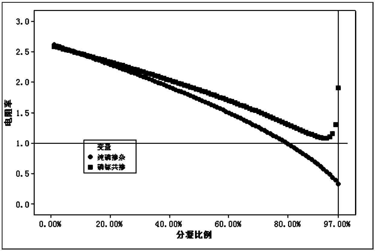
[0034] Step (1): Add the silicon raw material into the 28-inch quartz crucible placed in the main heating chamber of the single crystal furnace, and at the same time, put 30# phosphorus-based N-type master alloy and gallium in the middle part of the silicon raw material;

[0035] Step (2): Close the single crystal furnace, evacuate to below 40mtorr, conduct leak detection, heat and melt for 4.5H, then use the re-injector to re-inject silicon raw materials, and continue to heat and melt, specifically:

[0036] Vacuumize to below 40mtorr, automatic leak detection, leakage rate is lower than 40mtorr / h, the leak detection is considered qualified, start the pressure and fill the argon and vacuum valve, control the pressure in the furnace at 1600-2600pa, heat and melt, after melting for 4.5H , re-throw to the target weight, and continue to ...

Embodiment 2

[0045] A specific embodiment of a method for preparing solar-grade N-type single crystal silicon provided in this embodiment specifically includes the following steps:

[0046] Step (1): Add 250KG of solar super grade or electronic grade silicon raw material into a 28-inch quartz crucible placed in the main heating chamber of the single crystal furnace, and at the same time, put 30# phosphorus-based N-type master alloy 114 in the middle of the silicon raw material grams and gallium 1.5 grams;

[0047] Step (2): Close the single crystal furnace, evacuate to below 40mtorr, conduct leak detection, heat and melt for 4.5H, then re-inject 120KG of silicon raw material with a re-injector, and continue to heat and melt, specifically:

[0048] Vacuumize to below 40mtorr, automatic leak detection, leak detection is considered qualified if the leak rate is lower than 40mtorr / h, start pressure and fill with argon and vacuum valve, control the pressure in the furnace at 1600-2600pa, heat a...


PUM

PropertyMeasurementUnit
lengthaaaaaaaaaa

Abstract

A process for preparing solar-grade N-type monocrystalline is disclosed. The process includes (1) adding a silicon raw material into a quartz crucible put into a monocrystalline furnace, adding an N type master alloy and gallium to the middle position of the silicon raw material; (2) closing the monocrystalline furnace, vacuumizing the furnace to detect leakage, heating the furnace for a melting purpose, adding the silicon raw material with a repeated feeder and heating the furnace for a melting purpose; (3) cooling the furnace, stabilizing the temperature, finding out power, melting seed crystal, seeding, crowning, shouldering, bodying and tailing to obtain a first monocrystalline rod, pulling the monocrystalline rod to an auxiliary chamber of the monocrystalline furnace to be cooled, andmaintaining the temperature of the residual solution in the monocrystalline furnace; (4) taking the monocrystalline rod out after the monocrystalline rod is cooled and weighing the monocrystalline rod; (5) adding a material for repeated addition into the repeated feeder, and adding an N type master alloy and gallium to the middle position of the silicon raw material; and (6) heating the furnace for a melting purpose, cooling and stabilizing the furnace, finding out power, melting seed crystal, seeding, crowning, shouldering, bodying, tailing, and cooling the product to obtain a second monocrystalline rod. A proper amount of the gallium is added in the initial material addition to neutralize phosphorus better and to effectively improve the degree of centralization of the specific resistance of the N-type monocrystalline, thus increasing the percent of pass of solar resistance.

Description

technical field [0001] The invention relates to a method for preparing single crystal silicon, in particular to a method for preparing solar-grade N-type single crystal silicon, which belongs to the field of single crystal silicon and is used for resistance control of N-type single crystal silicon. Background technique [0002] Monocrystalline silicon solar cells have the characteristics of high efficiency and good stability. The efficiency of industrialized p-type monocrystalline silicon solar cells is generally between 20 and 21%. With the continuous improvement of solar cell efficiency requirements, the continuous development of battery technology , put forward higher requirements for monocrystalline silicon wafers, the efficiency of N-type monocrystalline silicon solar cells can reach 22%-23%, and the future high-efficiency cell technology must use N-type monocrystalline, for example, HII needs to use N-type monocrystalline At the same time, the commonly used boron-doped...

Claims


Application Information

Patent Timeline
Patent Type & Authority Applications(China)
IPC IPC(8): C30B15/04C30B15/20C30B29/06
CPCC30B15/04C30B15/20C30B29/06
Inventor 孟涛王海庆路景刚
Owner 包头美科硅能源有限公司
Why Eureka
Try Eureka