

A light-controlled neurosynaptic bionic electronic device and its preparation method
A technology of electronic devices and neural synapses, applied in electrical components, semiconductor devices, circuits, etc., can solve the problems of non-controllability, slow response, storage continuity, poor stability, etc., to achieve easy control, improve stability, low The effect of power consumption
- Summary
- Abstract
- Description
- Claims
- Application Information
AI Technical Summary
Problems solved by technology
Method used
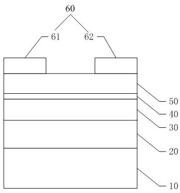
Image

Examples
preparation example Construction
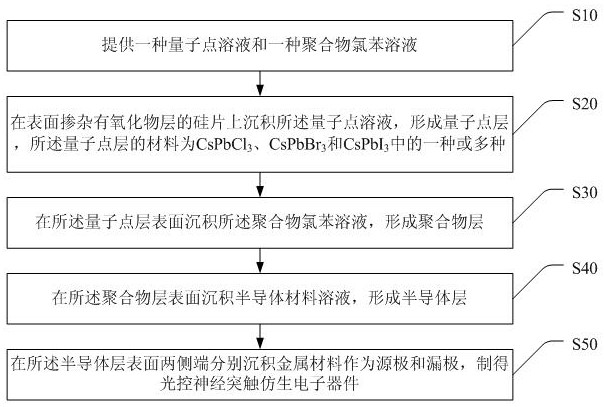
[0049] Based on the above-mentioned light-controlled synaptic bionic electronic device, the present invention also provides a preparation method of a light-controlled synaptic bionic electronic device, wherein, as figure 2 shown, including steps:
[0050] S10, providing a quantum dot solution and a polymer chlorobenzene solution;
[0051] S20, depositing the quantum dot solution on a silicon wafer doped with an oxide layer on the surface to form a quantum dot layer, the material of the quantum dot layer is CsPbCl 3 , CsPbBr 3 and CsPbI 3 one or more of
[0052] S30, depositing the polymer chlorobenzene solution on the surface of the quantum dot layer to form a polymer layer;
[0053] S40, depositing a semiconductor material solution on the surface of the polymer layer to form a semiconductor layer;
[0054] S50. Depositing metal materials on both sides of the surface of the semiconductor layer as source and drain respectively, so as to prepare a bionic electronic device ...
Embodiment 1
[0069] Fully mix cesium carbonate, octadecene and oleic acid in a nitrogen glove box, and heat to 150°C until the reaction is complete to form a cesium oleate solution;
[0070] Then mix lead chloride and octadecene fully and heat to 120°C, inject oleylamine and oleic acid in sequence, heat to 160°C after completely mixing and dissolving, then inject cesium oleate at 100°C, cesium oleate and chloride The molar ratio of lead is 5:1, ice bath after 5 seconds of reaction;
[0071] Using ethanol to make the prepared CsPbCl 3 Quantum dots were precipitated and redispersed in n-hexane solution to obtain inorganic halogen perovskite fluorescent quantum dots CsPbCl 3 solution.
[0072] Spin-coating CsPbCl on Si substrate doped with SiO2 3Quantum dot solution, followed by annealing at 100°C for 1h to form CsPbCl 3 quantum dot layer;
[0073] In CsPbCl 3 spin-coating polymethyl methacrylate solution on the quantum dot layer to form a polymer layer;
[0074] Pentacene organic smal...
Embodiment 2
[0077] Fully mix cesium carbonate, octadecene and oleic acid in a nitrogen glove box, and heat to 150°C until the reaction is complete to form a cesium oleate solution;
[0078] Then mix lead bromide and octadecene fully and heat to 120°C, inject oleylamine and oleic acid in sequence, heat to 160°C after completely mixing and dissolving, then inject cesium oleate at 100°C, cesium oleate and bromide The molar ratio of lead is 6:1, after 5 seconds of reaction, ice bath;
[0079] Using ethanol to make the prepared CsPbBr 3 Quantum dots were precipitated and redispersed in n-hexane solution to obtain inorganic halogen perovskite fluorescent quantum dots CsPbBr 3 solution.
[0080] Spin-coating CsPbBr on Al2O3-doped Si substrates 3 Quantum dot solution, followed by annealing at 120°C for 70min to form CsPbBr 3 quantum dot layer;
[0081] In CsPbBr 3 Spin coating polystyrene (PS) solution on the quantum dot layer to form a polymer layer;
[0082] Pentacene organic small molec...
PUM
| Property | Measurement | Unit |
|---|---|---|
| thickness | aaaaa | aaaaa |
| concentration | aaaaa | aaaaa |
| thickness | aaaaa | aaaaa |
Abstract
Description
Claims
Application Information