A back-passivated crystalline silicon solar cell and a preparation method thereof

A solar cell and backside passivation technology, applied in the field of solar cells, can solve the problems of reducing minority carrier lifetime, increasing cell cracks and cracks, increasing recombination centers, etc.

Active Publication Date: 2018-12-25
ZHEJIANG NORMAL UNIVERSITY
View PDF4 Cites 6 Cited by
  • Summary
  • Abstract
  • Description
  • Claims
  • Application Information

AI Technical Summary

Problems solved by technology

During the sintering process, the silver paste ablates the silicon matrix in the laser opening, which increases the recombination center and reduces the minority carrier lifetime, thus affecting the battery efficiency.
At the same time, the laser ablation on the back and the stress caused by the uneven aluminum back field greatly increase the probability of cell cracks and cracks
In addition, since the opening restricts the transport path of carriers, it deviates from the shortest path perpendicular to the contact surface and congests at the opening, which increases the loss of fill factor.

Method used


Image

  • A back-passivated crystalline silicon solar cell and a preparation method thereof
  • A back-passivated crystalline silicon solar cell and a preparation method thereof

Examples


Embodiment Construction

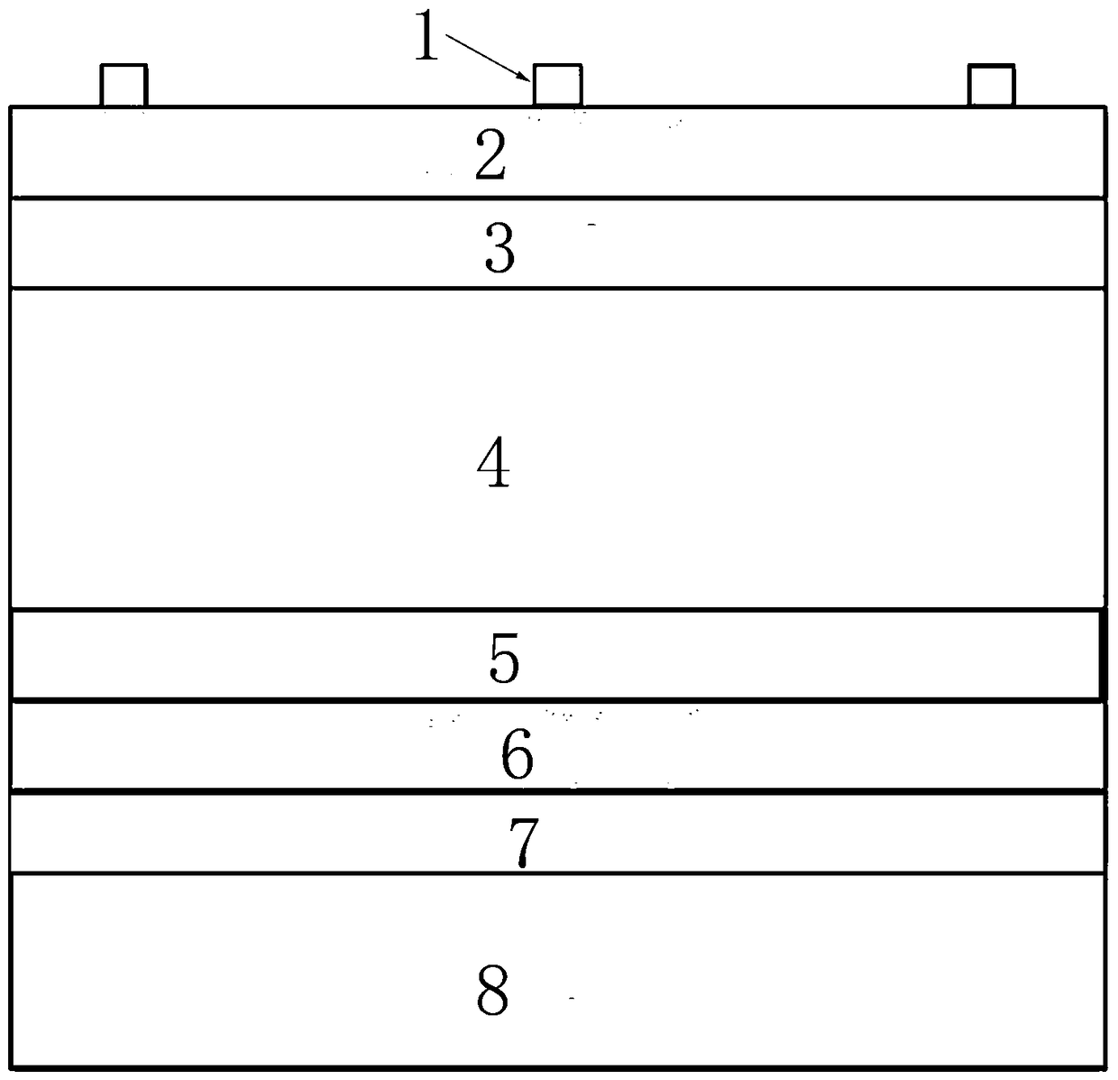
[0024] The crystalline silicon solar cell described in this embodiment uses molybdenum oxide as the p-type crystalline silicon passivation layer and the hole transport layer, and has the following structure: front Ag electrode 1, SiN x Layer (80nm) 2, n-c-Si layer 3, p-c-Si layer 4, SiO 2 Layer (1.2-1.5nm) 5, MoO 3 Layer (3nm) 6, Al layer (3nm) 7, back Ag electrode 8, wherein x=0.9-1.2, n-c-Si is phosphorus-doped n-type crystalline silicon.

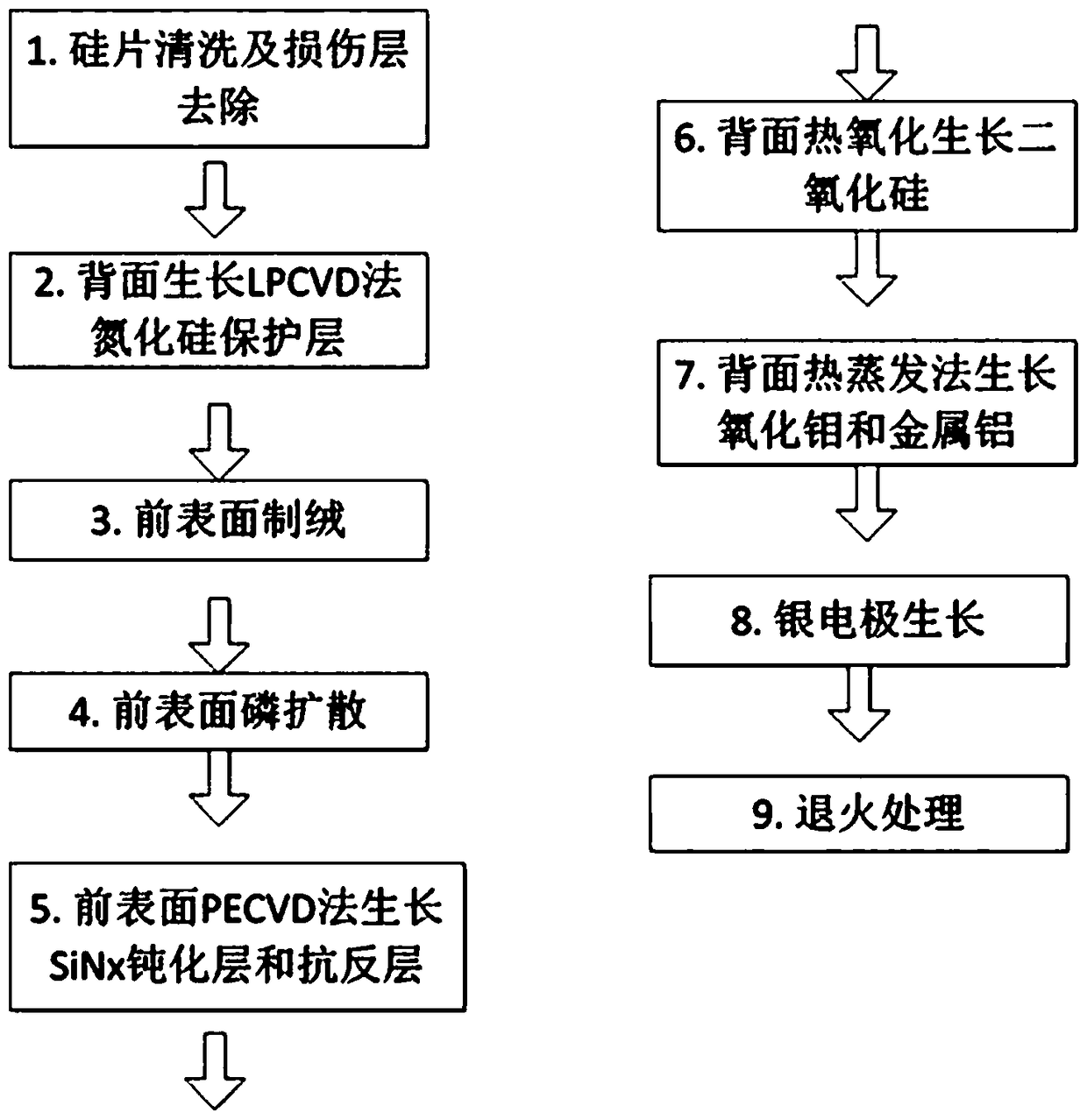
[0025] The preparation process of the battery is as follows:

[0026] 1) Cleaning and cashmere

[0027]The silicon wafer used in the experiment is a single crystal silicon wafer cut by diamond wire, with a resistivity of 0.5-1.5Ω.cm, a thickness of 180μm, and a size of 4×4cm. 2 . First, immerse the silicon wafer in acetone and absolute ethanol solution successively and use ultrasonic cleaning for 10 minutes to remove surface oil stains and dirt; secondly, treat the silicon wafer in a 30% sodium hydroxide solution at 80°C for 20 minute...


PUM

PropertyMeasurementUnit
electrical resistivityaaaaaaaaaa
thicknessaaaaaaaaaa
thicknessaaaaaaaaaa

Abstract

The invention discloses a back-passivated crystalline silicon solar cell and a preparation method thereof. Molybdenum oxide is used as a p-type crystalline silicon passivation layer and a hole transport layer, and the solar cell has the following structure: Ag / SiNx / n-C-Si / p-C-Si / SiO2 / MoO3 / Al / Ag, where x=0. 9-1.2, and n-C-Si is phosphorus doped n-type crystalline silicon. The invention uses molybdenum oxide instead of alumina as the back passivation material of the p-type crystalline silicon cell, and thus the recombination of the back side of the cell can be greatly reduced and the molybdenumoxide can also be used as the hole transport layer of the p-type crystalline silicon cell. Therefore, in the actual production process of the cell, the laser drilling is not required to ensure the transmission of carriers like PERC cells, which can not only reduce the backside recombination of crystalline silicon, but also avoid the negative impact of laser drilling.

Description

technical field [0001] The invention belongs to the field of solar cells, and in particular relates to a rear passivated crystalline silicon solar cell and a preparation method thereof. Background technique [0002] In solar cells, the separation, transport, and collection of photogenerated carriers are critical to improving the overall performance of the cell. Reducing the recombination of photogenerated carriers in the bulk and surface of crystalline silicon (c-Si) is crucial to improve the carrier collection efficiency, especially when the minority carrier diffusion length of the silicon wafer is comparable to or exceeds the thickness of the silicon wafer , the recombination on the surface of the silicon wafer has a much greater impact on the cell characteristics than the recombination in the body. Therefore, surface passivation is the key to the design and optimization of crystalline silicon solar cells. At present, silicon nitride film is used as the anti-reflection la...

Claims


Application Information

Patent Timeline
Patent Type & Authority Applications(China)
IPC IPC(8): H01L31/049H01L31/0216H01L31/18H01L31/0304
CPCH01L31/02167H01L31/03044H01L31/049H01L31/1876Y02E10/544Y02P70/50
Inventor 黄仕华周理想池丹陆肖励
Owner ZHEJIANG NORMAL UNIVERSITY
Why Eureka
Try Eureka