Large-area molecular crystal and preparation method thereof
What is AI technical title?
AI technical title is built by Patsnap AI team. It summarizes the technical point description of the patent document.
A molecular crystal, large-area technology, used in crystal growth, chemical instruments and methods, semiconductor/solid-state device manufacturing, etc. high uniformity
Active Publication Date: 2019-01-04
INST OF CHEM CHINESE ACAD OF SCI
View PDF6 Cites 6 Cited by
Summary
Abstract
Description
Claims
Application Information
AI Technical Summary
This helps you quickly interpret patents by identifying the three key elements:
Problems solved by technology
Method used
Benefits of technology
Problems solved by technology
Most of today's research focuses on inorganic materials such as boronnitride and transition metal chalcogenides. However, due to the difficulty of preparation, there are relatively few studies on organic two-dimensional semiconductors.
Method used
Image
Click on the blue label to locate the original text in one second.
Reading with bidirectional positioning of images and text.
Examples
Embodiment 1
[0039] Example 1, Preparation and Characterization of CMUT Monolayer Molecular Crystals
[0040] The CMUT used in this embodiment is according to the literature (Wu, Q.et al.Dicyanomethylene-Substituted Fused Tetrathienoquinoid for High-Performance, Ambient-Stable, Solution-Processable n-Channel Organic Thin-Film Transistors.Chem.Mater.23,3138-3140 (2011)) method synthesis.
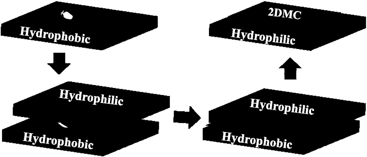
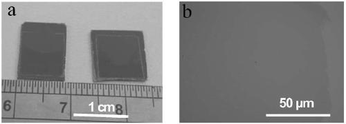
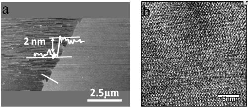
[0041] according to figure 1 As shown in the schematic diagram, a smaller-sized OTS hydrophobic substrate-modified oxide-doped siliconwafer is placed in a vessel at room temperature as a hydrophobic substrate, and an organic semiconductor with a volume concentration of 15 mg / mL is dripped on it. solution (the solvent is chlorobenzene), then cover it with an oxidation-doped siliconwafer whose size is slightly larger than that of the hydrophobic substrate as a hydrophilic substrate, and cover the vessel with a lid. After 12 hours, it was taken out, and a large-area organic semiconductor two-dimensional ...
Embodiment 2
[0045] Embodiment 2, device preparation
[0046] The CMUT organic semiconductor two-dimensional molecular crystal prepared in Example 1 was constructed into a field effecttransistor by using a method of transferring a gold film by a mechanical probe.
[0047] Figure 5 a and Figure 5 b are the transfer characteristic curve and output characteristic curve of the field effecttransistor with the CMUT two-dimensional molecular crystal structure, respectively. It can be seen that the mobility of the device can reach up to 2.8cm 2 V -1 the s -1 .
Embodiment 3
[0048] Example 3, Preparation and Characterization of HTEB Monolayer Molecular Crystals
[0049] The HTEB used in this embodiment is according to the literature (Meng, Q.et al.New Type of Organic Semiconductors for Field-Effect Transistors with Carbon-carbon Triple Bonds, Ambient-Stable, Solution-Processable n-Channel Organic Thin-FilmTransistors.J.Mater .Chem.19, 1477-1482 (2009)) method synthesis.
[0050] according to figure 1 As shown in the schematic diagram, a small BCB-modified oxide-doped siliconwafer is placed in a vessel at room temperature as a hydrophobic substrate, and an organic semiconductor solution with a volume concentration of 0.01 mg / mL is dripped on it. (the solvent is chlorobenzene), and then cover it with an oxidation-doped silicon wafer whose size is slightly larger than that of the hydrophobic substrate as a hydrophilic substrate, and cover the vessel lid. After 16 hours, it was taken out, and a large-area organic semiconductor two-dimensional molec...
PUM
Abstract
The invention discloses large-area molecular crystal and a preparation method thereof. The preparation method for the large-area molecular crystal comprises the following steps that an organic semiconductor solution is placed on a substrate with a hydrophobic property, a substrate with a hydrophily property covers the substrate with the hydrophobic property, and after growth, molecular crystal canbe obtained on the substrate with the hydrophily property; the organic semiconductor solution adopts at least one of chlorobenzenesolvent, trichloromethane solvent, dichlorobenzenesolvent and xylene solvent; the massvolume density of the organic semiconductor solution is 0.01 mg / mL-15 mg / mL; the solutes of the organic semiconductor solution are organic semiconductor molecules. The large-area molecular crystal has the advantages of a large area, high uniformity and a flat surface, a field effecttransistor prepared by the large-area two-dimensional molecular crystal has higher carrier mobility rate and lower thresholdvoltage, and solid foundation is laid for the preparation of later P-N heterojunction.
Description
technical field [0001] The invention relates to a large-area molecular crystal and a preparation method thereof, belonging to the technical field of organic semiconductor materials. Background technique [0002] Since the emergence of graphene, two-dimensional atomic crystals have attracted extensive attention. Most of the current research focuses on inorganic materials such as boronnitride and transition metal chalcogenides. However, due to the difficulty of preparation, there are relatively few studies on organic two-dimensional semiconductors. It is well known that large-area two-dimensional molecular crystals (2DMC) can construct high-performance transistors, which are expected to exceed the mobility of self-assembled monolayers bonded to substrates, which are generally lower than 0.05 cm 2 V -1 the s -1 . Large-area 2D transistors can reduce the bulk resistance and reduce the exposure of the semiconductor charge accumulation layer. This low defect density provides ...
Claims
Application Information
Patent Timeline
Application Date:The date an application was filed.
Publication Date:The date a patent or application was officially published.
First Publication Date:The earliest publication date of a patent with the same application number.
Issue Date:Publication date of the patent grant document.
PCT Entry Date:The Entry date of PCT National Phase.
Estimated Expiry Date:The statutory expiry date of a patent right according to the Patent Law, and it is the longest term of protection that the patent right can achieve without the termination of the patent right due to other reasons(Term extension factor has been taken into account ).
Invalid Date:Actual expiry date is based on effective date or publication date of legal transaction data of invalid patent.

