A near-room temperature preparation process of high performance thin film transistor and application

A thin-film transistor and fabrication process technology, applied in transistors, semiconductor/solid-state device manufacturing, semiconductor devices, etc., can solve problems such as the inability to prepare fully transparent devices, the difficulty of precise control of film thickness, and the inability to be compatible with flexible plastic substrates. , to achieve the effect of good optical response characteristics, excellent electrical characteristics, and precise and controllable thickness

Active Publication Date: 2019-01-04
FUDAN UNIV
View PDF5 Cites 5 Cited by
  • Summary
  • Abstract
  • Description
  • Claims
  • Application Information

AI Technical Summary

Problems solved by technology

This makes them incompatible with flexible plastic substrates
[0004] Plasma enhanced chemical vapor deposition (PECVD) technology can prepare gate dielectric film at 90°C, but due to its fast reaction rate, the thickness of the film is difficult to control precisely, and the grown f

Method used


Image

  • A near-room temperature preparation process of high performance thin film transistor and application
  • A near-room temperature preparation process of high performance thin film transistor and application
  • A near-room temperature preparation process of high performance thin film transistor and application

Examples


Embodiment

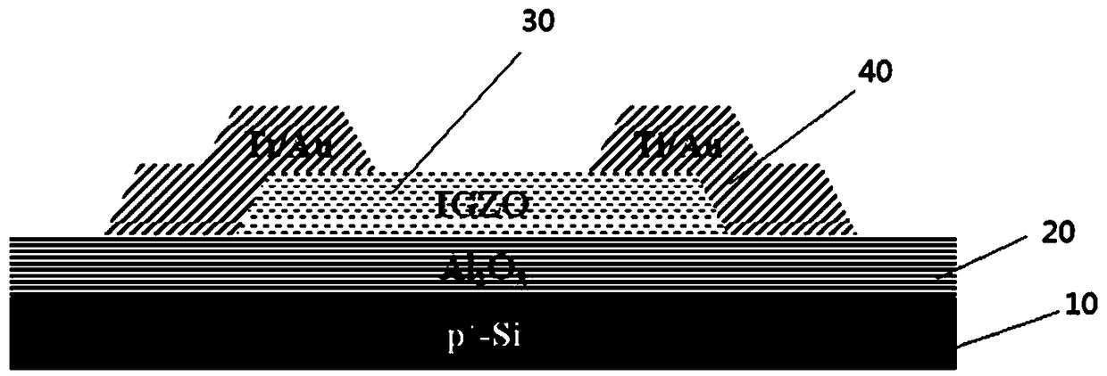
[0028] Put the heavily doped P-type Si substrate 10 into the ALD reaction chamber, and deposit Al at 30°C 2 o 3 Gate insulating layer 20, its thickness is 40nm; Will grow Al 2 o 3 The Si substrate of the gate insulating layer is placed in the magnetron sputtering deposition chamber, and the IGZO layer 30 is grown at near room temperature with a thickness of 40nm. Then the obtained device is processed in a clean room. Firstly, the first photolithography is carried out to make the photoresist form a channel pattern on the surface of the film, and then a dilute hydrochloric acid solution is arranged to etch the IGZO film to form a channel, and then acetone is used to remove residual photoresist on the surface. Then the second photolithography was carried out, and the negative gel was uniformly coated on the surface of the sample, and then exposed under the exposure machine for 30 seconds, and then developed with a negative gel developer to form a source-drain electrode pattern...


PUM

PropertyMeasurementUnit
Thicknessaaaaaaaaaa
Thicknessaaaaaaaaaa
Thicknessaaaaaaaaaa

Abstract

The invention discloses a near-room temperature preparation process of a high-performance thin film transistor and application. The process comprises the following steps: 1, placing a conductive substrate into an atomic layer deposition reaction chamber and vacuumizing; 2, depositing and growing Al2O3 at 20-40 DEG C; 3, put that device obtained in the step 2 into a magnetron sputter deposition cavity and vacuumizing; 4, grow an IGZO channel layer under the temperature of 20 to 40 DEG C; 5, carrying out ultraviolet exposure on the device obtained in the step 4, and etching to form a channel; 6,perform second photolithography, evaporating a source-drain electrode, remove photoresist, and obtaining a bottom gate type high-performance thin film transistor without annealing treatment. The invention provides a near-room temperature preparation process of a high-performance thin film transistor, and the thin film transistor has the responsiveness to light of different wavelengths and can beused in the fields of flexible electronics, photoelectric detection, bioelectronics and the like.

Description

technical field [0001] The invention belongs to the field of semiconductor devices, and in particular relates to a near-room-temperature preparation process of a high-performance thin film transistor and its application. Background technique [0002] In recent years, flexible electronics technology has attracted widespread attention due to its excellent flexibility, lightness and portability, low process cost, and large-area manufacturing. It has shown great application potential in information fields such as flexible displays, smart wear, and medical electronics. . How to directly fabricate thin film transistor (Thin film transistor, TFT) devices on flexible substrates has become the key to this technology. This requires that the temperature of the fabrication process should be reduced as much as possible during the fabrication of the TFT device. The main technical difficulty lies in how to obtain high-quality gate dielectric film under low temperature conditions. [000...

Claims


Application Information

Patent Timeline
IPC IPC(8): H01L29/786H01L21/285H01L21/34
CPCH01L21/285H01L29/66742H01L29/78693H01L29/78696
Inventor 丁士进邵龑刘文军张卫
Owner FUDAN UNIV
Why Eureka
Try Eureka