A lateral MOS type power semiconductor device and a preparation method thereof

A technology of power semiconductors and semiconductors, applied in semiconductor/solid-state device manufacturing, semiconductor devices, electrical components, etc., can solve problems such as increased cost, increased chip area, and increased power consumption

Active Publication Date: 2019-01-08
UNIV OF ELECTRONICS SCI & TECH OF CHINA
View PDF5 Cites 6 Cited by
  • Summary
  • Abstract
  • Description
  • Claims
  • Application Information

AI Technical Summary

Problems solved by technology

For traditional LDMOS (such as figure 1 Shown) and LIGBT devices, if you want to increase the withstand voltage capability of the device, you must increase the length of the drift region to improve the withstand voltage capability of the device, but this will increase the on-resistance / on-voltage drop of the device and increase the power consumption , the chip area increases and the cost increases
Although the industry introduces the effect of double reducing the surface electric field (RESURF) in the drift region, the improvement of device performance is very limited.

Method used


Image

  • A lateral MOS type power semiconductor device and a preparation method thereof
  • A lateral MOS type power semiconductor device and a preparation method thereof
  • A lateral MOS type power semiconductor device and a preparation method thereof

Examples


Embodiment 1

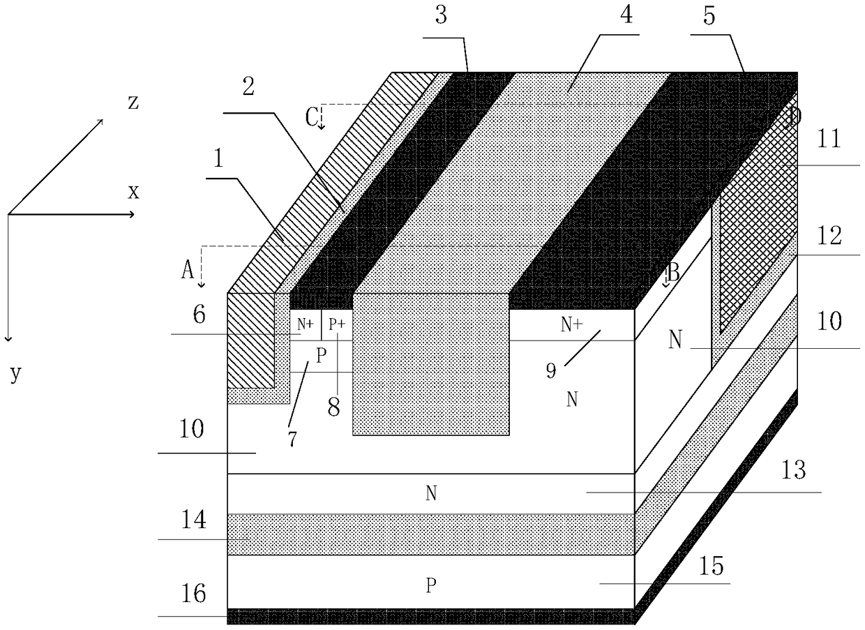
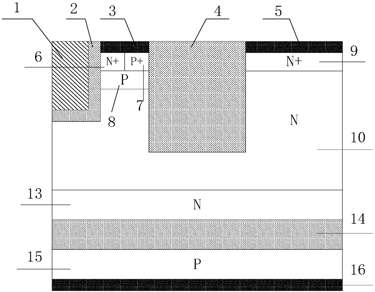
[0086] This embodiment provides an LDMOS device, the cell structure of which is as follows figure 2 as shown, figure 2 The schematic diagrams of the cross-sectional structure of the cellular structure along the AB line and the CD line are shown in Fig. image 3 and 4 shown, combined with Figures 2 to 4 From the point of view, the cellular structure includes: a substrate electrode 16 stacked vertically from bottom to top, a P-type semiconductor layer 15, a buried oxide layer 14, an N-type buffer layer 13, and an N-type drift region 10; the N-type drift region 10 One side of the surface is provided with an N-type drain region 9; the other side of the surface of the N-type drift region 10 is provided with a MOS structure, and the MOS structure includes a P-type body region 7, an N+ source region 6, a P+ contact region 8, a trench gate Structure and source electrode 3, wherein the trench gate structure includes a trench gate electrode 1 and a trench gate dielectric layer 2 a...

Embodiment 2

[0090] This embodiment provides an LDMOS device, the cell structure of which is as follows Figure 5 as shown, Figure 5 The schematic diagrams of the cross-sectional structure of the cell structure along the AB line, CD line and EF line are shown in Fig. Figure 6 , 7 and 8, combined with Figures 5 to 8 From the point of view, this embodiment is based on Embodiment 1, and a P-type column region 17 is provided on the side of the N-drift region 10 relatively away from the semi-insulating polysilicon column 11, and the lower surface of the P-type column region 17 is connected to the N-type column region. - the buffer layer 13 is in contact; the P-type pillar regions 17 are parallel to the N-drift regions 10 along the lateral extension direction of the deep dielectric trench 4 and are arranged alternately to form a super junction structure. In this embodiment, the width of the P-type column region 17 along the z-axis direction is 0.5-1.5 μm, the longitudinal depth along the y...

Embodiment 3

[0092] This embodiment provides an LDMOS device, the cell structure of which is as follows Figure 9 as shown, Figure 9 The schematic diagrams of the cross-sectional structure of the cell structure along the AB line, CD line and EF line are shown in Fig. Figure 10 , 11 As shown in and 12, this embodiment is based on embodiment 2, in the N-type drift region 10 and the P-type column region 17 below the N-type drain region 9, the side N close to the side wall of the deep dielectric trench 4 is set. The doping concentration of the N-type buffer layer 18 on the side is not less than the doping concentration of the N-type drift region 10 . The doping concentration of the side N-type buffer layer 18 can be uniform doping, or decreasing from top to bottom. The introduction of the side N-type buffer layer 18 can suppress the influence of auxiliary depletion on the charge balance between the N-type drift region 10 and the P-type column region 17 due to the different potentials on b...


PUM


Abstract

The invention provides a transverse MOS device and a preparation method thereof, belonging to the technical field of semiconductor power devices. The invention introduces a deep dielectric trench, a semi-insulating polysilicon column and a buffer layer into the drift region of a conventional transverse MOS type device. The introduction of deep dielectric trench makes the device form U-shaped conductive channel, which effectively increases the length of drift region under the same device length. A 3-D resistive field plate structure is for by alternately connecting that semi-insulating polysilicon column and the drift region along the transverse extension direction of the deep dielectric trench so as to introduce a multi-dimensional depletion action in the drift region when the device is blocked to increase the doping concentration of the drift region, The drift region width on both sides of the deep trench is not limited by the doping dose, which improves the electric field distribution in the drift region, increases the breakdown voltage of the device and reduces the specific on-resistance/on-voltage drop of the device. The introduction of buffer layer can improve the charge balance characteristics of three-dimensional dielectric superjunction structure, and further improve the performance and reliability of the device.

Description

technical field [0001] The invention belongs to the technical field of power semiconductor devices, and in particular relates to a lateral MOS type power semiconductor device and a preparation method thereof. Background technique [0002] With the rapid development of electronic technology, there is an urgent demand for high-voltage integrated power MOS devices. Lateral double diffused metal oxide semiconductor field effect transistor (LDMOS) and lateral insulated gate bipolar transistor (LIGBT) devices are widely used in In large-scale integrated circuits, it has become an indispensable part of the development of power integrated circuits. For traditional LDMOS (such as figure 1 Shown) and LIGBT devices, if you want to increase the withstand voltage capability of the device, you must increase the length of the drift region to improve the withstand voltage capability of the device, but this will increase the on-resistance / on-voltage drop of the device and increase the powe...

Claims


Application Information

Patent Timeline
Patent Type & Authority Applications(China)
IPC IPC(8): H01L29/78H01L29/739H01L29/10H01L29/06H01L21/336H01L21/331
CPCH01L29/063H01L29/1033H01L29/66325H01L29/66704H01L29/7393H01L29/7394H01L29/7812H01L29/7825
Inventor 张金平王康罗君轶赵阳刘竞秀李泽宏张波
Owner UNIV OF ELECTRONICS SCI & TECH OF CHINA
Why Eureka
Try Eureka