Method for preparing graphene single crystal wafer at low temperature

A technology of graphene and single crystals, which is applied in the field of low-temperature preparation of graphene single crystal wafers, can solve the problems of graphene single crystal wrinkles, achieve good crystallinity, consistent orientation, and reduce wrinkles

Active Publication Date: 2019-01-15
SHANGHAI INST OF MICROSYSTEM & INFORMATION TECH CHINESE ACAD OF SCI
View PDF3 Cites 5 Cited by
  • Summary
  • Abstract
  • Description
  • Claims
  • Application Information

AI Technical Summary

Problems solved by technology

[0003] The technical problem to be solved by the present invention is to provide a method for preparing graphene single crystal wafers at low temperature, so as to overcome the defect of wrinkles in the graphene single crystal prepared at high temperature in the prior art

Method used


Image

  • Method for preparing graphene single crystal wafer at low temperature
  • Method for preparing graphene single crystal wafer at low temperature
  • Method for preparing graphene single crystal wafer at low temperature

Examples


Embodiment 1

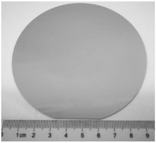
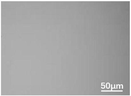
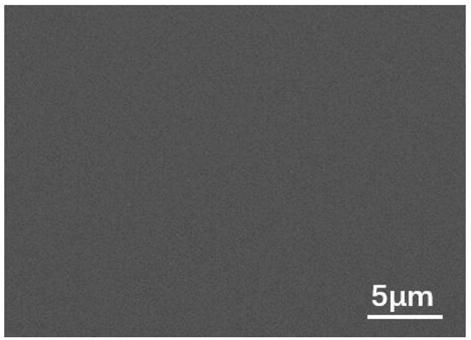
[0037] Sapphire was selected as the substrate, and nickel-copper alloy thin films were prepared by magnetron sputtering. The sputtering is carried out under the conditions of high-purity argon gas and a vacuum of 0.5 Pa, and the sputtering rate is 5 nm / min. A 50nm copper-nickel alloy substrate is deposited on the surface of a sapphire substrate (at a temperature of 50° C.) by magnetron sputtering, wherein the content of nickel element is 5%. The film is placed in a chemical vapor deposition system, and annealed in an argon and hydrogen protective atmosphere, wherein the flow rate of argon and hydrogen is 400sccm: 10sccm, the annealing temperature is 750°C, the annealing time is 60min, and then 10sccm methane is introduced , grown for 60 min, and grown under normal pressure to obtain a graphene single crystal wafer. By Raman (eg Figure 5 Shown) It can be seen that the quality of graphene is relatively high, and there are no defect peaks in the Raman peak of graphene.

[003...

Embodiment 2

[0044] Change the copper-nickel alloy substrate in embodiment 1 to a copper-platinum alloy substrate, wherein the platinum element content is 5%, the growth temperature is changed to 600 ° C, and the rest of the process parameters are the same as in embodiment 1 to obtain a graphene single crystal wafer, Raman spectrum such as Image 6 As shown, it can be seen that at ~1600cm -1 And ~ 2700cm -1 Graphene characteristic peak appears at 1400cm -1 No defect peaks were found at , confirming that the quality of the grown graphene is relatively high.

[0045] Figure 10 It shows that there are six bright points in the figure, indicating that the graphene is in the same orientation and is single crystal graphene.

Embodiment 3

[0047] Change the copper-nickel alloy substrate in Example 1 to a copper-palladium alloy substrate, wherein the palladium element content is 10%, the growth temperature is changed to 500 ° C, and the growth pressure is 10 -10 Pa, the carbon source is changed into ethylene, and all the other process parameters are identical with embodiment 1, obtain graphene single crystal wafer, and Raman collection of illustrative plates is as follows Figure 7 As shown, it can be seen that at ~1600cm -1 And ~ 2700cm -1 Graphene characteristic peak appears at 1400cm -1 No defect peaks were found at , confirming that the quality of the grown graphene is relatively high.

[0048] Figure 11 It shows that the graphene spots are six-fold symmetric and have the same orientation, which is a graphene single crystal.


PUM

PropertyMeasurementUnit
thicknessaaaaaaaaaa

Abstract

The invention relates to a method for preparing a graphene single crystal wafer at low temperature, and the method comprises: depositing a layer of binary copper-based alloy thin film on the surface of a single crystal insulating substrate, placing the alloy thin film in a chemical vapor deposition system for annealing treatment, introducing a gaseous carbon source, and epitaxially growing the graphene single crystal wafer at the low temperature. According to the method, wrinkles of graphene are reduced, the electrical property of the graphene is further improved, and the production cost of the graphene single crystal wafer is reduced.

Description

technical field [0001] The invention belongs to the field of material preparation, in particular to a method for preparing graphene single crystal wafers at low temperature. Background technique [0002] The unique properties of graphene have attracted widespread attention from people from all walks of life. Its excellent optoelectronic properties are expected to be widely used in the field of microelectronics in the future, becoming another host material after silicon materials. The preparation of wafer-scale graphene single crystals is the prerequisite for its large-scale application in the field of microelectronics in the future. The temperature required for the existing graphene single crystal growth technology is relatively high. The difference in thermal expansion coefficient between graphene and the substrate causes large wrinkles in graphene after cooling down. These wrinkles greatly reduce the electrical properties of graphene single crystal. Performance, and high...

Claims


Application Information

Patent Timeline
Patent Type & Authority Applications(China)
IPC IPC(8): C01B32/188
CPCC01B32/188
Inventor 张学富王浩敏吴天如于庆凯谢晓明
Owner SHANGHAI INST OF MICROSYSTEM & INFORMATION TECH CHINESE ACAD OF SCI
Why Eureka
Try Eureka