A semiconductor heterojunction photocatalytic material and its preparation method and application

A photocatalytic material and heterojunction technology, applied in chemical instruments and methods, physical/chemical process catalysts, metal/metal oxide/metal hydroxide catalysts, etc., can solve the problem of fast electron and hole recombination, photo Reduced efficiency of catalytic capacity, reduced active carriers and other issues, to achieve the effect of wide source of raw materials, low cost, and improved activity efficiency

Active Publication Date: 2021-07-20
NANTONG TEXTILE & SILK IND TECH RES INST +1
View PDF4 Cites 0 Cited by
  • Summary
  • Abstract
  • Description
  • Claims
  • Application Information

AI Technical Summary

Problems solved by technology

[0003] In recent years, oxide-based catalyst materials have been widely studied and applied, such as typical photocatalyst representatives: titanium dioxide (TiO 2 ), zinc oxide (ZnO), cadmium sulfide (CdS), bismuth oxide (Bi 2 o 3 ), tungsten oxide (WO 3 ) and so on, as potential photocatalytic materials, although photocatalytic research has been carried out for several years, these materials still have some shortcomings, such as: narrow spectral response range, poor stability, low photoconversion efficiency, etc., so there is an urgent need for research and development new photocatalyst
The study found that the most important disadvantage of many oxide photocatalyst materials currently being studied is that the recombination speed of electrons and holes is too fast, which greatly reduces the active carriers participating in photocatalysis, resulting in a decrease in the efficiency of photocatalysis.

Method used


Image

  • A semiconductor heterojunction photocatalytic material and its preparation method and application
  • A semiconductor heterojunction photocatalytic material and its preparation method and application
  • A semiconductor heterojunction photocatalytic material and its preparation method and application

Examples


Embodiment 1

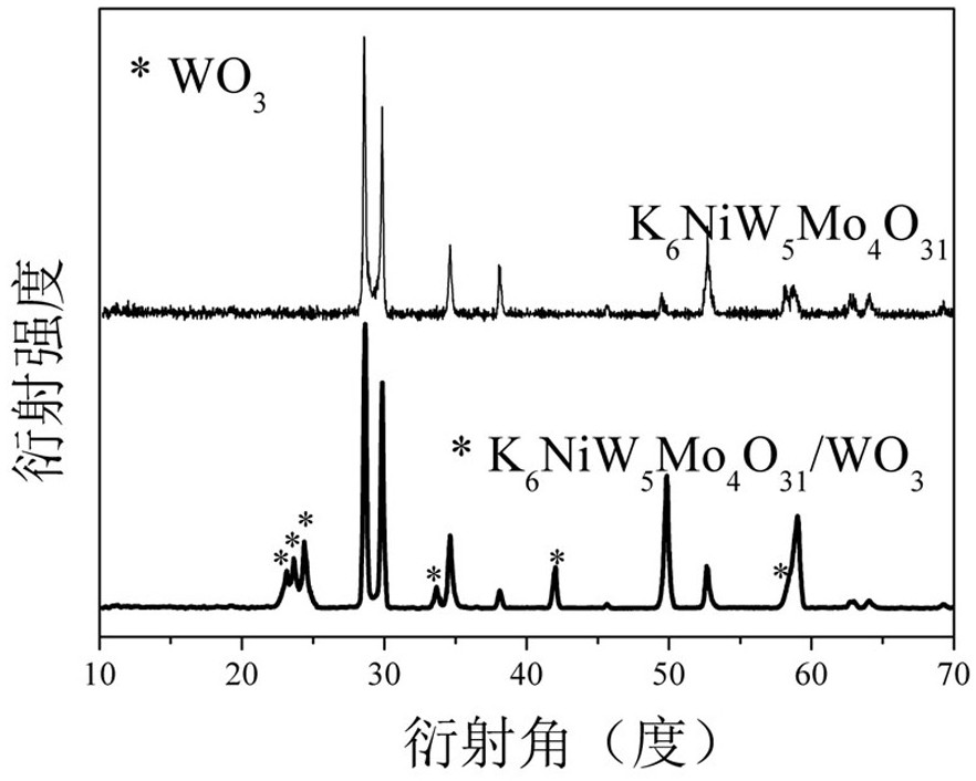
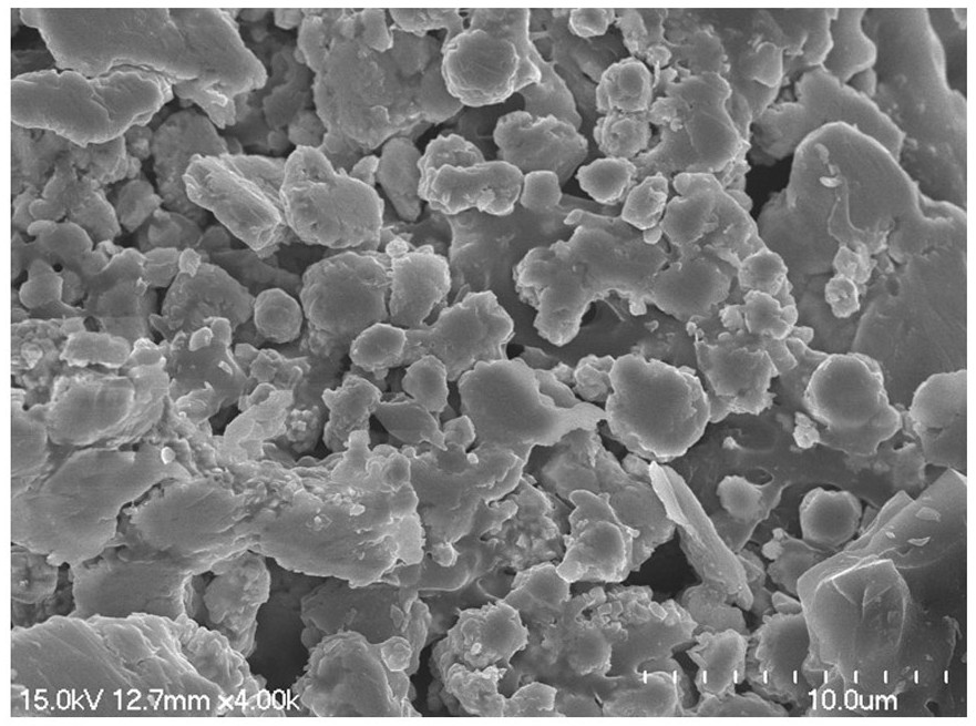
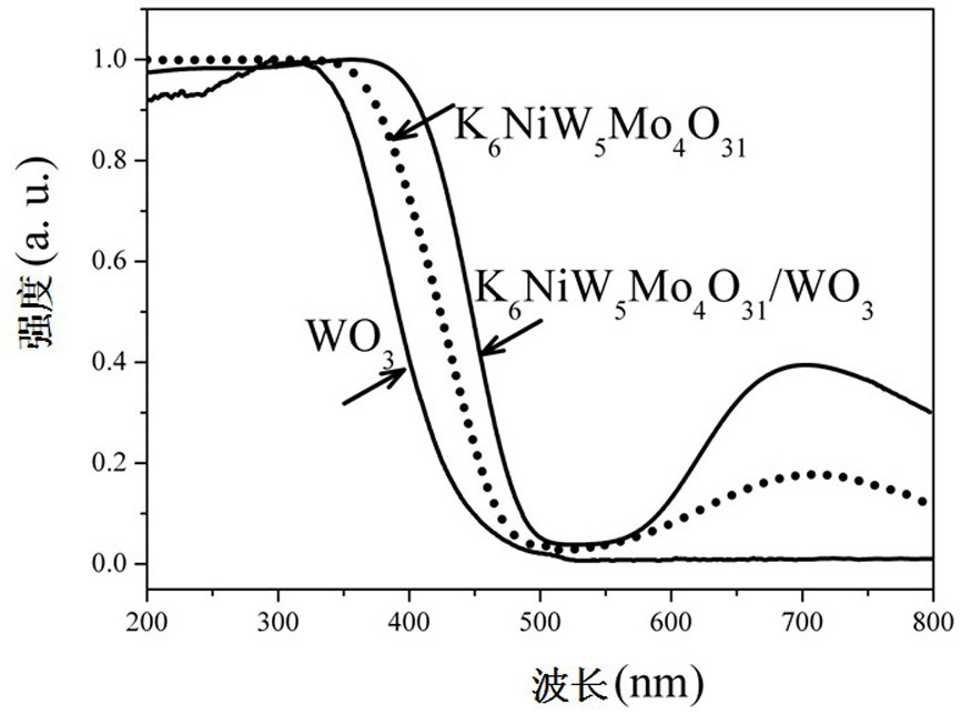
[0032] According to chemical formula K 6 NiW 5 Mo 4 o 31 The stoichiometric ratio of each element in the formula, respectively weigh potassium oxide K 2 O: 0.942 grams, nickel oxide NiO: 0.2490 grams, ammonium tungstate (NH 4 ) 6 W 7 o 24 ·6H 2 O: 7.24 g, ammonium molybdate (NH 4 ) 6 Mo 7 o 24 4H 2 O: 2.352 grams, after grinding and mixing in an agate mortar, pre-calcined in an air atmosphere, the calcination temperature is 550 ° C, the calcination time is 10 hours, after natural cooling, grind to make it evenly mixed, and then calcined in an air atmosphere , the calcination temperature is 950°C, the calcination time is 1 hour, cooled naturally, and the precursor K is obtained after uniform grinding 6 NiW 5 Mo 4 o 31 .

[0033] will get K 6 NiW 5 Mo 4 o 31 Precursor and tungsten oxide 1.16 g WO 3 Mix by ball milling, and the ball milling time is 20 hours. The mixture obtained by ball milling was calcined in the air atmosphere, the calcining temperature w...

Embodiment 2

[0040] According to chemical formula K 6 NiW 5 Mo 4 o 31 The stoichiometric ratio of each element in the formula, respectively weigh potassium carbonate K 2 CO 3 : 2.76 grams, nickel oxide NiO: 0.497 grams, tungsten oxide WO 3 : 7.73 g, ammonium molybdate (NH 4 ) 6 Mo 7 o 24 4H 2 O: 4.69g, after grinding and mixing uniformly in an agate mortar, pre-calcined in air atmosphere, the calcination temperature is 850°C, the calcination time is 1 hour, after natural cooling, grind to make it evenly mixed, and then calcined in air atmosphere , the calcination temperature was 850°C, the calcination time was 5 hours, cooled naturally, and the precursor K was obtained after uniform grinding 6 NiW 5 Mo 4 o 31 .

[0041] will get K 6 NiW 5 Mo 4 o 31 Precursor with tungsten oxide 0.25 g WO 3 Mix by ball milling, and the ball milling time is 1 hour. The mixture obtained by ball milling was calcined in the air atmosphere, the calcining temperature was 600°C, the calcining t...

Embodiment 3

[0043] According to chemical formula K 6 NiW 5 Mo 4 o 31 The stoichiometric ratio of each element in the formula, respectively weigh potassium carbonate K 2 CO 3 : 1.38 g, nickel nitrate Ni (NO 3 ) 2 ·6H 2 O: 0.97 g, ammonium tungstate (NH 4 ) 6 W 7 o 24 ·6H 2 O: 8.69 g, ammonium molybdate (NH 4 ) 6 Mo 7 o 24 4H 2 O: 2.822g, after grinding and mixing uniformly in an agate mortar, pre-calcining in air atmosphere, the calcination temperature is 700°C, the calcination time is 3 hours, after natural cooling, grind to make it evenly mixed and then calcined in air atmosphere , the calcination temperature was 850°C, the calcination time was 7 hours, cooled naturally, and the precursor K was obtained after uniform grinding 6 NiW 5 Mo 4 o 31 .

[0044] Weigh 7.61 grams of ammonium tungstate (NH 4 ) 6 W 7 o 24 ·6H 2 O was dissolved in 50 ml distilled water, and the resulting K 6 NiW 5 Mo 4 o 31 The precursor was added to the solution, heated and stirred at ...


PUM

PropertyMeasurementUnit
particle sizeaaaaaaaaaa

Abstract

The invention discloses a semiconductor heterojunction photocatalytic material, a preparation method and application thereof. K provided by the present invention 6 NiW 5 Mo 4 o 31 / WO 3 semiconductor heterojunction, in K 6 NiW 5 Mo 4 o 31 is the precursor substrate material, K 6 NiW 5 Mo 4 o 31 with WO 3 The molar ratio is 100:(5~50). The semiconductor heterojunction photocatalytic material provided by the present invention can be synthesized by a high-temperature solid-phase method or a chemical solution method. The preparation method is simple and easy, the material has good chemical stability, can effectively absorb ultraviolet-visible light, and can achieve high efficiency under visible light. photocatalytic activity. and single-phase precursor substrate material K 6 NiW 5 Mo 4 o 31 Compared with heterojunction composite catalysts, it can better absorb visible light, effectively realize electron-hole separation, improve catalytic efficiency, and can be used for photocatalytic degradation of organic pollutants, especially for organic dye industrial wastewater Visible light catalytic degradation treatment.

Description

technical field [0001] The invention relates to a semiconductor heterojunction photocatalytic material and its preparation method and application, belonging to the field of inorganic photocatalytic materials. Background technique [0002] With the rapid development of modern society and industry, the extensive use of the three major fossil fuels has brought serious resource shortages and environmental pollution, which seriously restricts and threatens the development of human society. Pay attention to. Among them, photocatalytic technology based on semiconductor oxides has become an important means of controlling environmental pollution due to its excellent properties such as no pollution, simple process, and rapid response to sunlight. Photocatalytic technology is the basic photochemical technology born in the 1970s. Japanese scientists Fujishma and Honda reported in 1972 that titanium dioxide can be used as a photoanode to decompose H under the condition of ultraviolet li...

Claims


Application Information

Patent Timeline
Patent Type & Authority Patents(China)
IPC IPC(8): B01J23/888C02F1/30C02F101/30
CPCB01J23/8885B01J35/004C02F1/30C02F2101/308
Inventor 黄彦林刘宣宣米龙庆魏东磊
Owner NANTONG TEXTILE & SILK IND TECH RES INST
Why Eureka
Try Eureka