A nitrogen doping method for preparing low COP defect silicon single crystal

A technology of silicon single crystal and nitrogen doping, which is applied in the directions of single crystal growth, single crystal growth, diffusion/doping, etc., can solve the problems of weak silicon single crystal COP defect suppression and poor nitrogen doping effect, etc., to achieve Low heating power, reduced production cost, and high dissociation efficiency

Active Publication Date: 2021-01-12
CHINA ELECTRONICS TECH GRP NO 46 RES INST
View PDF6 Cites 0 Cited by
  • Summary
  • Abstract
  • Description
  • Claims
  • Application Information

AI Technical Summary

Problems solved by technology

[0005] In view of the above-mentioned analysis of the technical problems in the prior art, the present invention aims to provide a nitrogen doping method for preparing silicon single crystals with low COP defects, in order to solve the poor effect of nitrogen doping in the prior art and the COP of silicon single crystals. Technical problems with weak suppression of defects

Method used


Image

  • A nitrogen doping method for preparing low COP defect silicon single crystal
  • A nitrogen doping method for preparing low COP defect silicon single crystal
  • A nitrogen doping method for preparing low COP defect silicon single crystal

Examples


Embodiment 1

[0031] Embodiment 1: The nitrogen doping method for preparing low COP defect silicon single crystal has the following steps:

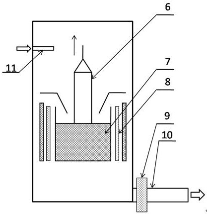
[0032] (1) if image 3 As shown, an ammonia gas high-temperature ionization device 11 is added in the middle of the Czochralski method silicon single crystal furnace chamber; during the growth process of the Czochralski method silicon single crystal 6, high-purity ammonia gas is passed into the ammonia gas high-temperature dissociation device to generate N( g), the ammonia flow rate is 0.03SLM. In this embodiment, the temperatures of the inlet area, middle area, and outlet area of ​​the heater are set as follows: 1250°C, 1150°C, and 1050°C.

[0033] (2) N (g) dissolves in the silicon melt 7 and diffuses to the solid-liquid interface of the single crystal growth, and then enters the interior of the silicon single crystal as the growth process progresses to realize the nitrogen doping process and inhibit the silicon single crystal Crystalline COP defec...

Embodiment 2

[0036] Embodiment 2: The nitrogen doping method for preparing low COP defect silicon single crystal has the following steps:

[0037] Such as Figure 4 As shown, the difference between this embodiment and Embodiment 1 is that an ammonia gas high-temperature ionization device 11 is added at the lower part of the chamber of the Czochralski silicon single crystal furnace, that is, near the position of the graphite heater; this embodiment sets the heater inlet The temperature of the area, the middle area, and the outlet area are as follows: 850°C, 750°C, and 650°C.

[0038] Since the ammonia gas high-temperature ionization device 11 is placed near the graphite heater 8, the high-temperature ionization process of ammonia gas can be completed by the heating effect of the graphite heater 8. Therefore, compared with embodiment 1, this embodiment can significantly reduce the heating rate. The heating power of the device.


PUM


Abstract

The invention discloses a nitrogen doping method for preparing low-COP defect silicon single crystal. The method comprises the following steps: adding an ammonia gas high-temperature dissociation device during the process of Czochralski silicon single crystal growth, feeding high-purity ammonia gas into the ammonia gas high-temperature dissociation device to produce N(g), dissolving the N(g) intosilicon melt, diffusing the silicon melt to a single crystal growth solid and liquid interface, and then entering the silicon single crystal along with the growth process, so as to realize a nitrogendoping process and inhibit silicon single crystal COP defects. Compared with the traditional nitrogen gas atmosphere nitrogen doping method, the method has the advantages that the nitrogen gas dissociation temperature is low, the dissociation efficiency is high, the nitrogen doping effect is easy to realize, and Czochralski low-COP defect silicon single crystal is easy to prepare. Low nitrogen gasdissociation temperature signifies lower heating efficiency, and high nitrogen gas dissociation temperature signifies little required gas sources, so that the method greatly reduces the production cost, and can be applied to volume production of Czochralski low-COP defect silicon single crystal.

Description

technical field [0001] The invention relates to the preparation technology of semiconductor single crystal silicon material, in particular to a nitrogen doping method for preparing low COP defect silicon single crystal. Background technique [0002] Semiconductor single crystal silicon material is the basic material of electronic industry such as semiconductor device and integrated circuit. From the perspective of improving the yield of silicon devices and integrated circuits and reducing costs, increasing the diameter of silicon single crystals is still the development trend of Czochralski silicon single crystal preparation technology in the future. Crystal Originated Particles (Crystal Originated Particles) defects, referred to as COP defects, often exist in large-diameter Czochralski silicon single crystals. When the size of the COP defect reaches the scale of the characteristic line width, it will seriously affect the integrity of the gate oxide layer of the integrated ...

Claims


Application Information

Patent Timeline
Patent Type & Authority Patents(China)
IPC IPC(8): C30B15/04C30B29/06C30B31/06
CPCC30B15/04C30B29/06C30B31/06
Inventor 张颖武韩焕鹏赵堃李明佳莫宇张伟才赵权刘锋
Owner CHINA ELECTRONICS TECH GRP NO 46 RES INST
Why Eureka
Try Eureka