Two-dimensional superlattice indium selenide and preparation method and application thereof in fabrication of photoelectric detector

A photodetector and superlattice technology, applied in circuits, electrical components, semiconductor/solid-state device manufacturing, etc., can solve the problems of low light detection performance and poor electrical transport performance of two-dimensional semiconductor materials, and achieve high light response, The effect of good photoelectric detection performance and good application prospect

Inactive Publication Date: 2019-03-01
NORTHEAST FORESTRY UNIVERSITY
View PDF6 Cites 12 Cited by
  • Summary
  • Abstract
  • Description
  • Claims
  • Application Information

AI Technical Summary

Problems solved by technology

[0004] The present invention solves the technical problems of poor electrical transport performance of existing two-dimensional semiconductor materials and low photodetection performance of photodetectors, and provides a preparation method of two-dimensional superlattice indium selenide and its application in the preparation of photodetectors. application in

Method used


Image

  • Two-dimensional superlattice indium selenide and preparation method and application thereof in fabrication of photoelectric detector
  • Two-dimensional superlattice indium selenide and preparation method and application thereof in fabrication of photoelectric detector
  • Two-dimensional superlattice indium selenide and preparation method and application thereof in fabrication of photoelectric detector

Examples


Embodiment 1 2

[0034] The preparation of embodiment 1 two-dimensional superlattice InSe

[0035] Step 1, SiO with a thickness of 300nm 2 The / Si substrate was ultrasonically treated with isopropanol, acetone, ethanol and ultrapure water at 10KHz in sequence, and the ultrasonic treatment time was 10min, dried with nitrogen, and set aside;

[0036] Step 2: Paste the bulk InSe material 6 times with scotch tape at basically the same position, and then paste the scotch tape on the 300nm SiO2 treated in step 1 2 / SiO on Si substrate 2 8 hours on one side, after removing the scotch tape, the SiO 2 / Si substrate soaked in acetone for 3 hours, remove the SiO 2 / Si substrate can obtain randomly distributed two-dimensional InSe nanosheets on its surface;

[0037] Step three, the SiO 2 / Si substrate is placed in a tube furnace, the tube furnace is evacuated to 80Torr, and 100sccmAr / H is introduced 2 The mixed gas (V Ar :V H2 =80:20), the furnace temperature was raised to 350°C in 17.5 minutes,...

Embodiment 2 2

[0038] Embodiment 2 Preparation of two-dimensional superlattice InSe photodetector

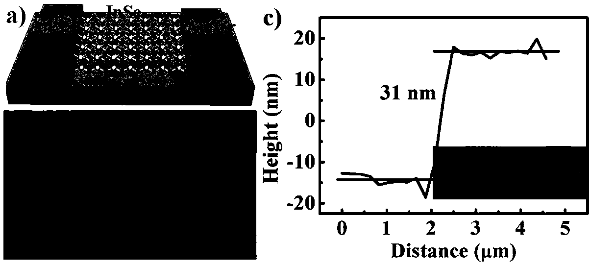
[0039] Select the 300nm SiO prepared in Example 1 2 2D superlattice InSe nanosheets with a lateral size of 50 microns and a thickness of 31nm on the surface of the Si substrate, using silver glue to fix the metal mask to cover the center of the two-dimensional superlattice InSe nanosheets, leaving two sides on each side. Dimensional superlattice InSe nanosheets with a width of 3 μm were placed in a vacuum coating machine at a vacuum degree of 3×10 -4 Under the condition of Pa, the two-dimensional superlattice InSe photodetector can be obtained by sequentially vapor-depositing 5nm metallic chromium and 40nm metallic gold electrodes on one side of the two-dimensional superlattice InSe nanosheet.

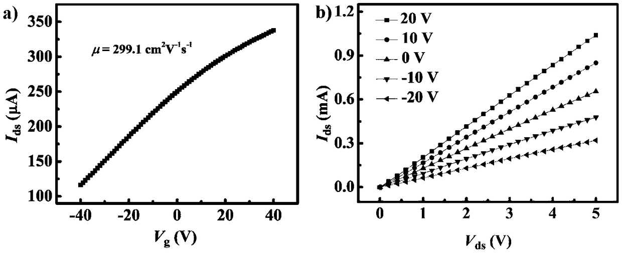
[0040] The detection of 700nm excitation light by the two-dimensional superlattice InSe photodetector of this embodiment:

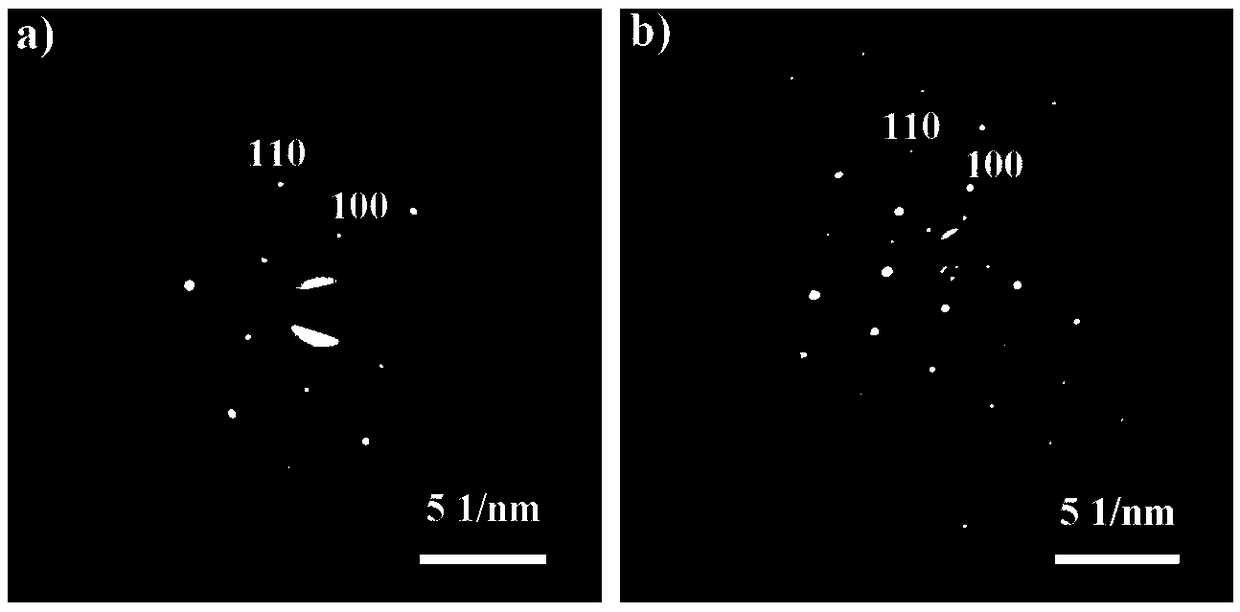
[0041] In this embodiment, two-dimensional superlattice InSe nanosheets are...


PUM

PropertyMeasurementUnit
thicknessaaaaaaaaaa
sizeaaaaaaaaaa
thicknessaaaaaaaaaa

Abstract

The invention discloses two-dimensional superlattice indium selenide and preparation method and application thereof in fabrication of a photoelectric detector, and belongs to the field of a high-performance photoelectric detector. The fabrication method of the two-dimensional superlattice indium selenide comprises the steps of pre-processing a SiO2/Si substrate; transferring onto the SiO2/Si substrate after an InSe material is pasted with transparent glue, and immersing in acetone; and performing high-temperature processing under a vacuum condition, thereby obtaining a two-dimensional superlattice InSe nanosheet on a surface of the SiO2/Si substrate. The two-dimensional superlattice InSe prepared by the invention has the advantages of high electrical transmission performance, high light response, favorable stability and rapid light response speed and has a good application prospect in the field of the high-performance photoelectric detector.

Description

technical field [0001] The invention belongs to the field of high-performance photodetectors; in particular, it relates to two-dimensional superlattice indium selenide, its preparation method and its application in preparing photodetectors. Background technique [0002] A photodetector is a device that converts optical signals into electrical signals. It has great application prospects in the fields of optical communication, optical imaging, environmental monitoring, missile monitoring and remote control. It is a hot research field in the scientific community and has attracted scientists. Widespread attention and rapid development. Semiconductor materials with good light-absorbing ability and electrical properties are the basis for designing and preparing high-performance photodetectors. Photodetectors based on traditional semiconductor materials (silicon, gallium nitride, and indium gallium arsenide) exhibit small photodetection performance, with photoresponse values ​​les...

Claims


Application Information

Patent Timeline
Patent Type & Authority Applications(China)
IPC IPC(8): H01L21/02B82Y40/00
CPCB82Y40/00H01L21/02521H01L21/0259
Inventor 冯伟刘赫于苗苗秦芳璐
Owner NORTHEAST FORESTRY UNIVERSITY
Why Eureka
Try Eureka