

Synthesis device and synthesis method for NbSe2 monocrystal layered nanosheet
A synthesis device and synthesis method technology, applied in the direction of single crystal growth, single crystal growth, nanotechnology, etc., can solve the problems of low yield of nanosheets, cumbersome process, equipment damage, etc., and achieve simple preparation method, good repeatability, The effect of improving productivity efficiency
- Summary
- Abstract
- Description
- Claims
- Application Information
AI Technical Summary
Problems solved by technology
Method used
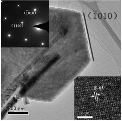
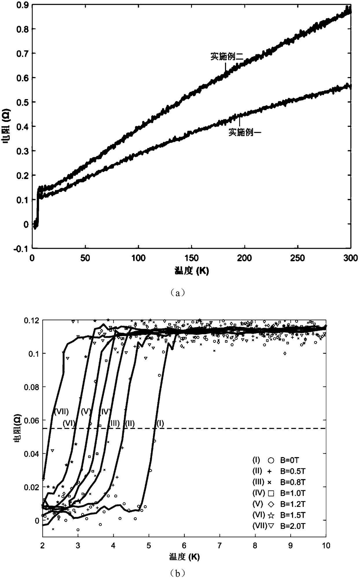
Image

Examples
Embodiment 1
[0034] The NbSe of this embodiment 2 The synthetic method of single-crystal layered nanosheet, comprises the following steps:
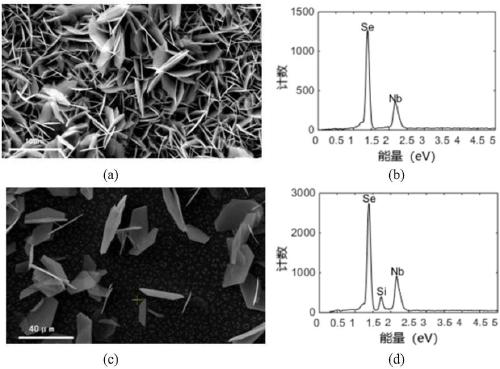
[0035] 1) Place 2.261g iodine source on the carrier gas source slide, 0.015gNbSe 2 The powder source is placed on the reactant carrier near the end of the carrier gas source carrier, and 8 silicon wafer deposition substrates are placed on the other end of the reactant carrier far away from the carrier gas source carrier. The side length of the silicon wafer deposition substrate is 5mm, arranged in order with the spacing between adjacent deposition substrates as 4mm, the distance between the silicon wafer deposition substrates and NbSe 2 The closest distance to the powder source is 16.1cm;
[0036] 2) Place the carrier gas source slide and the reactant slide in the sealed reactor along the length direction, the centerlines of the two are on the same straight line, the iodine source and the NbSe 2 The distance between the powder sources is 20cm, and ...
Embodiment 2
[0042] The NbSe of this embodiment 2 The synthetic method of single-crystal layered nanosheet, comprises the following steps:
[0043] 1) Place 3.227g iodine source on the carrier gas source slide, 0.024g NbSe 2 The powder source is placed on the reactant carrier near the end of the carrier gas source carrier, and 8 silicon wafer deposition substrates are placed on the other end of the reactant carrier far away from the carrier gas source carrier. The side length of the silicon wafer deposition substrate is 5mm, arranged in order with the spacing between adjacent deposition substrates as 4mm, the distance between the silicon wafer deposition substrates and NbSe 2 The closest distance to the powder source is 16cm;
[0044] 2) Place the carrier gas source slide and the reactant slide in the sealed reactor along the length direction, the centerlines of the two are on the same straight line, the iodine source and the NbSe 2 The distance between the powder sources is 20.4cm, and...
Embodiment 3
[0050] The NbSe of this embodiment 2 The synthetic method of single-crystal layered nanosheet, comprises the following steps:
[0051] 1) Place 3.183g iodine source on the carrier gas source slide, 0.022g NbSe 2 The powder source is placed on the reactant carrier near the end of the carrier gas source carrier, and the six silicon wafer deposition substrates are placed on the reactant carrier at the other end away from the carrier gas source carrier. The side length of the silicon wafer deposition substrate is 5mm, arranged in order with the spacing between adjacent deposition substrates as 6mm, the distance between the silicon wafer deposition substrates and NbSe 2 The closest distance to the powder source is 16.8cm;
[0052] 2) Place the carrier gas source slide and the reactant slide in the sealed reactor along the length direction, the centerlines of the two are on the same straight line, the iodine source and the NbSe 2 The distance between the powder sources is 19.8cm,...
PUM
 Abstract
Description
Claims
Application Information