Silicon crystal heterojunction solar cell and preparation method thereof

A solar cell and heterojunction technology, applied in the field of solar cells, can solve the problems of limiting the hole transport performance of the film and the limited control of the stoichiometric ratio of oxides, so as to reduce the density of defect states and the surface recombination rate of carriers, Improve the carrier transport capacity of the thin film and improve the effect of short-circuit current of the battery

Active Publication Date: 2019-04-12
HEBEI UNIVERSITY
View PDF5 Cites 2 Cited by
  • Summary
  • Abstract
  • Description
  • Claims
  • Application Information

AI Technical Summary

Problems solved by technology

This method requires high-vacuum equipment and has very limited control over the stoichiometric ratio of oxides, which limits the hole-transporting performance of the film to some extent.

Method used


Image

  • Silicon crystal heterojunction solar cell and preparation method thereof

Examples


Embodiment 1

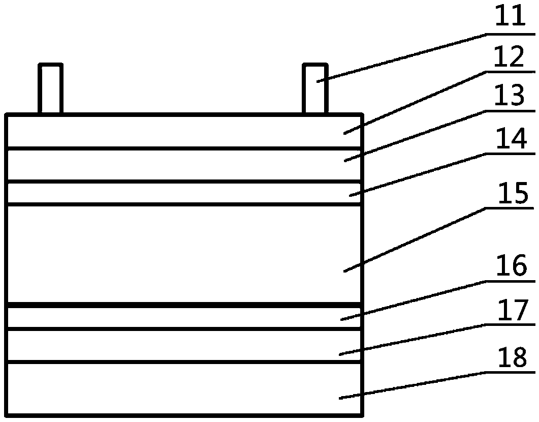
[0025] Such as figure 1 As shown, the present embodiment is based on the crystalline silicon heterojunction solar cell of the molybdenum oxysulfur hole extraction layer, and its structure is: a first tunneling layer 14, MoO 3-x S x The hole extraction layer 13 , the transparent conductive electrode 12 and the metal grid line 11 are sequentially prepared on the back of the n-type silicon wafer 15 with a second tunneling layer 16 , an electron extraction layer 17 and a metal back electrode 18 .

[0026] This embodiment specifically gives the preparation method of crystalline silicon heterojunction solar cells, as follows:

[0027] (1) The n-type CZ 180 micron (1~10 Ω·cm) silicon wafer was cleaned by RCA, and then the silicon wafer was immersed in diluted hydrofluoric acid (5%, 3 minutes) to remove the natural oxide layer on the surface. Put the cleaned silicon wafer into 70wt% nitric acid for 15 minutes (at room temperature) to form a tunnel oxide layer with a thickness of abo...

Embodiment 2

[0033] The difference between this example and Example 1 is that the molybdenum oxysulfur monolayer film structure is prepared in step (4) of Example 1, and the molybdenum oxysulfur / molybdenum oxide double layer is prepared in step (4) in this example structure, the two-layer structure together serves as a hole-extracting layer.

[0034] The preparation process of the molybdenum oxysulfide / molybdenum oxide double-layer structure is as follows: first evaporate molybdenum oxide with a thickness of 0.5nm to 5nm, and then deposit a molybdenum oxysulfide thin film by co-evaporating molybdenum sulfide and molybdenum oxide according to the method in Example 1.

Embodiment 3

[0036] Same as Example 1, the molybdenum oxysulfur monolayer thin film structure is also prepared in step (4) in this example, but the preparation method of the molybdenum oxysulfur single layer thin film structure in this example is as follows: molybdenum sulfide and molybdenum oxide are alternately Deposition, the evaporation rate of molybdenum oxide is 0.01~0.05nm / s, the evaporation rate of molybdenum sulfide is 0.01~0.1nm / s, and finally annealed, the annealing temperature is 100~300°C.


PUM

PropertyMeasurementUnit
Thicknessaaaaaaaaaa
Thicknessaaaaaaaaaa
Thicknessaaaaaaaaaa

Abstract

The invention provides a silicon crystal heterojunction solar cell and a preparation method thereof. The structure of the silicon crystal heterojunction solar cell comprises a metal grid, a transparent conductive electrode, an oxygen molybdenum sulfur-containing hole leading-out layer, a first tunneling layer, a silicon wafer, a second tunneling layer, an electronic leading-out layer and a metal back electrode, wherein the oxygen molybdenum sulfur-containing hole leading-out layer can be a MoO<3-x>S<x> single-layer thin film structure and also can be a MoO<3-x>S<x> / MoO3 dual-layer thin film structure, and for the MoO<3-x>S<x> / MoO3 dual-layer thin film structure, a MoO3 layer is contacted with the first tunneling layer. With the oxygen molybdenum sulfur-containing hole leading-out layer-based heterojunction solar cell prepared by the method, the defect state density and the carrier surface recombination rate of the material can be effectively reduced, and the short-circuit current of the cell and a built-in electric field are improved; and the hole selectivity is adjustable by the oxygen molybdenum sulfur-containing hole leading-out layer, and the fabrication process is simple and has relatively high industrial promotion and application value.

Description

technical field [0001] The invention relates to the technical field of solar cells, in particular to a crystalline silicon heterojunction solar cell and a preparation method thereof. Background technique [0002] In recent years, the photovoltaic industry has focused on finding crystalline silicon (c-Si) solar cell technology with the advantage of low-cost manufacturing. Strategies to reduce costs include using ultra-thin wafers or lower-quality substrates, but in any case lower material consumption and simplified manufacturing processes are required. [0003] Transition metal oxides (TMOs) as selective contact layers for electrons or holes have attracted extensive attention in the research of high-efficiency crystalline silicon cells. TMO is a wide range of work function (Φ TMO =3~7 eV) and wide bandgap (E g >3 eV) semiconducting materials that offer great flexibility when used as electron- or hole-selective contact materials. High work function V 2 o 5 、WO 3 、MoO...

Claims


Application Information

Patent Timeline
IPC IPC(8): H01L31/032H01L31/0216H01L31/074H01L31/18
CPCH01L31/02167H01L31/032H01L31/074H01L31/18H01L31/1804H01L31/1868Y02E10/547Y02P70/50
Inventor 于威刘海旭路万兵焦玉骁辛利桃许贺菊傅广生
Owner HEBEI UNIVERSITY
Why Eureka
Try Eureka