

TSV rapid filling method and device
A filling method and fast technology, applied in the direction of electrolysis components, electrolysis processes, circuits, etc., can solve the problems of TSV voids or slits, limited improvement capacity, filling defects, etc., to promote nucleation growth, improve production efficiency, and accelerate deposition. effect of speed
- Summary
- Abstract
- Description
- Claims
- Application Information
AI Technical Summary
Problems solved by technology
Method used
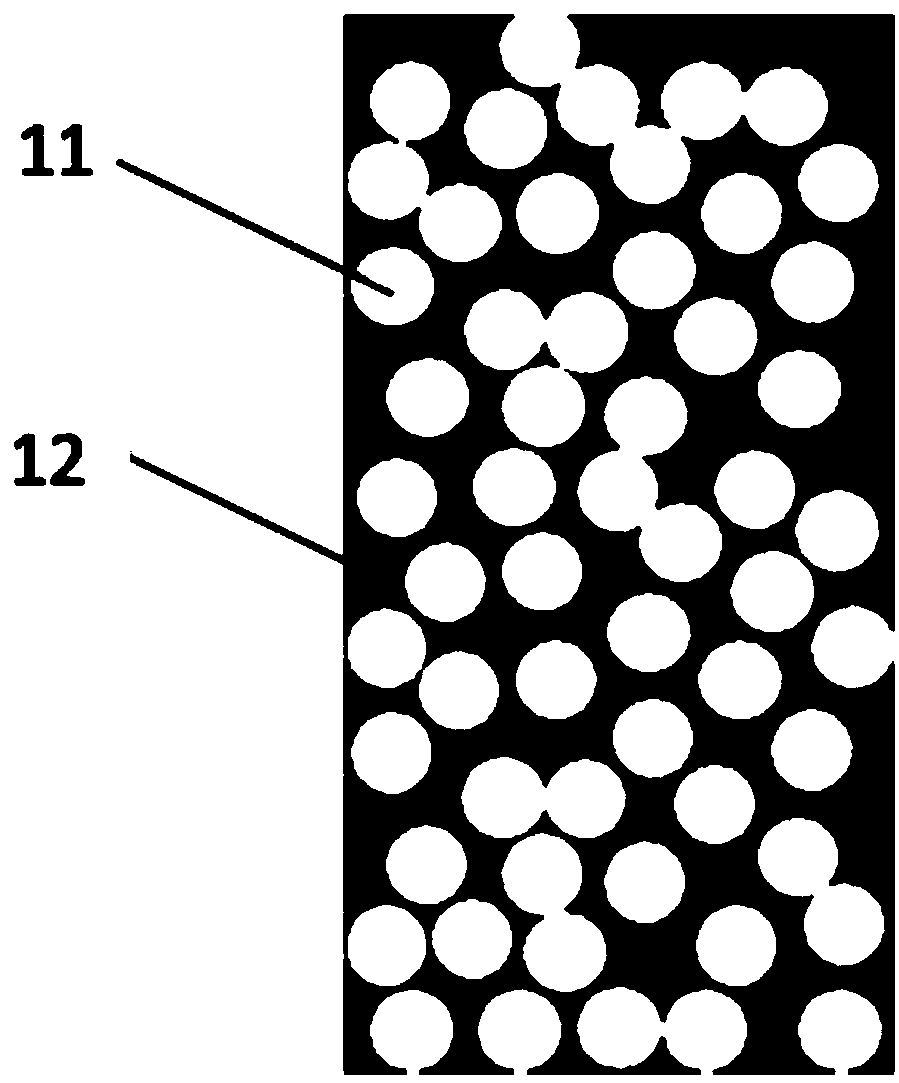
Image

Examples
Embodiment 1
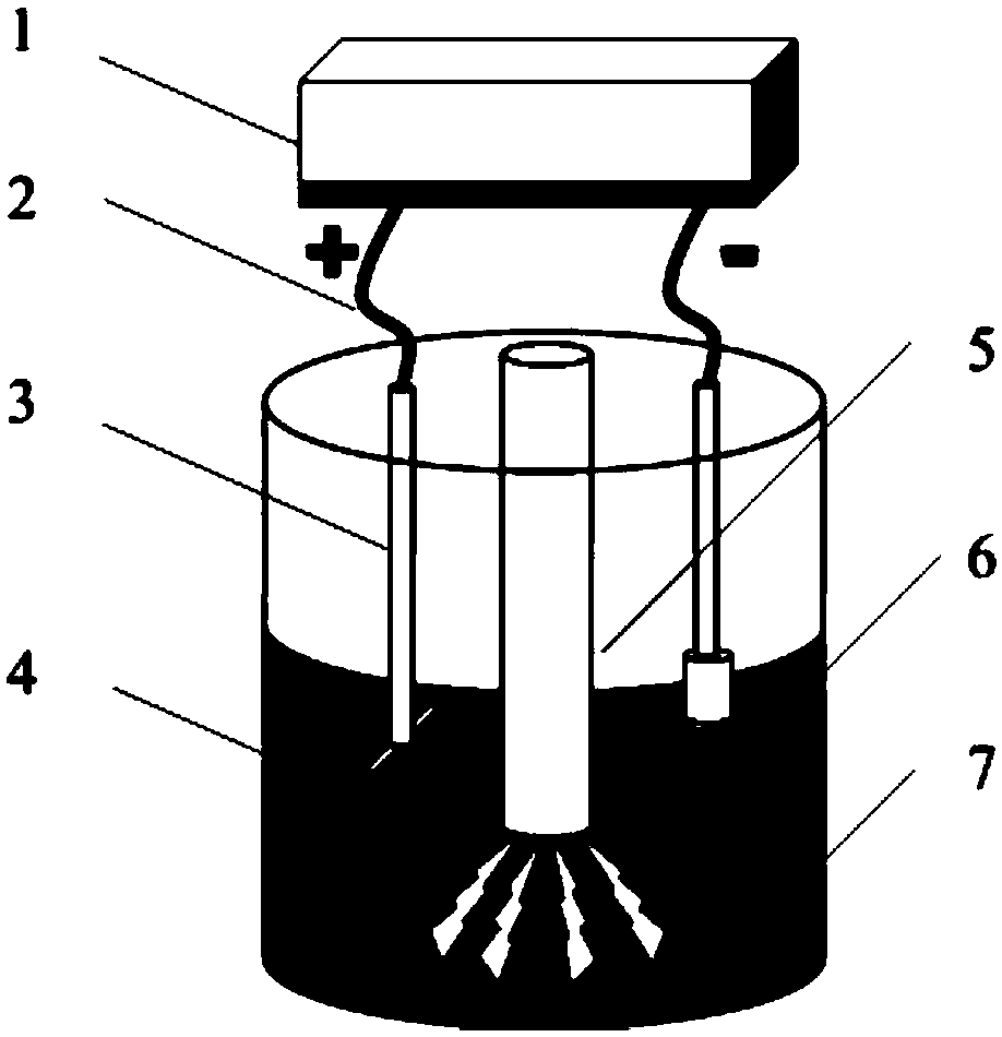
[0029] The TSV rapid filling device provided by the present invention, such as figure 2 As shown, including electroplating anode, electroplating cathode, electroplating power supply, electroplating solution and ultrasonic horn. The upper end of the electroplating anode is connected to the positive pole of the electroplating power supply through a wire, and the lower end is fixed in the electroplating solution by an electrode clamp; the upper end of the electroplating cathode is connected to the negative pole of the electroplating power supply through a wire, and the lower end is fixed in the electroplating solution by an electrode clamp; the ultrasonic horn and the electroplating Liquid contact for applying ultrasonic excitation. Wherein, the electroplating anode is a copper anode; the electroplating solution is a copper-containing electroplating solution, including a copper sulfate electroplating solution or a copper sulfonate electroplating solution.
Embodiment 2
[0031] The TSV fast filling method provided in this embodiment includes the following steps:
[0032] The first step: preparing a suspension containing silver nanoparticles;
[0033] Weigh 0.5g of nano-silver powder and pour it into a beaker, wherein the average particle size of the nano-silver is 20 nanometers; then measure 50ml of ethanol and pour it into the beaker, and stir fully to fully disperse and suspend the nano-silver particles in the ethanol solvent. A suspension of 10 g / L silver nanoparticles was obtained.
[0034] The second step: put the silicon chip and make the nano-silver particles precipitate into the TSV blind hole;
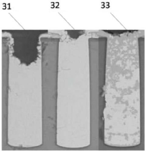
[0035] Cut out a silicon wafer containing TSV blind holes, wherein the size of the silicon wafer is 1cm in length and 2cm in width, and the size of the TSV blind hole is 20 μm in diameter and 65 μm in depth; the silicon wafer is washed with deionized water and put into the nano-silver suspension obtained in step 1 In the solution, keep the o...
Embodiment 3
[0044] The TSV fast filling method provided in this embodiment includes the following steps:
[0045] The first step: preparing a suspension containing nickel nanoparticles;
[0046] Weigh 0.4g of nano-nickel powder and pour it into a beaker, wherein the average particle size of nano-nickel is 20 nanometers; then measure 50ml of ethanol and pour it into the beaker, and stir fully to fully disperse and suspend the nano-nickel particles in the ethanol solvent. A suspension of 8 g / L nickel nanoparticles was obtained.
[0047] The second step: put the silicon wafer and precipitate the nano-nickel particles into the TSV blind hole;
[0048] Cut out a silicon wafer containing TSV blind holes, where the size of the silicon wafer is 1 cm long and 2 cm wide, and the size of the TSV blind hole is 20 μm in diameter and 65 μm in depth; the silicon wafer is washed with deionized water and put into the nano-nickel suspension obtained in step 1 Keep the opening of the TSV hole facing up; p...
PUM
| Property | Measurement | Unit |
|---|---|---|
| Depth | aaaaa | aaaaa |
Abstract
Description
Claims
Application Information