A substrate etching method for GAAS-based LED wafers
A substrate and wafer technology, applied in semiconductor devices, electrical components, circuits, etc., can solve problems such as thermal stress mismatch, reduction of effective light-emitting area, lattice mismatch, etc.
- Summary
- Abstract
- Description
- Claims
- Application Information
AI Technical Summary
Problems solved by technology
Method used
Image
Examples
Embodiment Construction
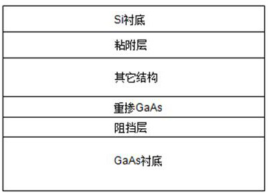
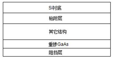
[0038] Such as figure 1 As shown, the GaAs-based LED wafer mentioned in the present invention before substrate etching is sequentially GaAs substrate, barrier layer (GaInP), heavily doped GaAs layer, "other structures", adhesion layer and Replace with Si substrate. "Other structures" at least include the P-type electrode structure formed by the metal layer, the barrier layer to prevent the interdiffusion of the P-type electrode metal and the adhesion layer metal, P-type GaAs layer, N-type GaAs layer and quantum well layer, etc. The metal used for the adhesion layer may be Au, Al, Ni, Ag, Sn or In and the like.
[0039] The present invention is figure 1 The method for etching the substrate of the GaAs-based LED wafer shown, such as figure 2 shown, including the following steps:
[0040] (1) GaAs substrate corrosion:
[0041] ① Prepare a mixed solution of ammonia water and hydrogen peroxide, the solution volume ratio, ammonia water: hydrogen peroxide = 1:5 ~ 1:7; put it in...
PUM
| Property | Measurement | Unit |
|---|---|---|
| thermal conductivity | aaaaa | aaaaa |
Abstract
Description
Claims
Application Information


