Manufacturing method of silicon detector array device for enhancing blue light efficiency

A detector array and manufacturing method technology, applied in semiconductor devices, electrical components, circuits, etc., can solve the problem of low blue light sensitivity, achieve uniform electric field distribution, improve quantum efficiency, and reduce photosensitive area

Active Publication Date: 2019-04-30
CHANGCHUN INST OF OPTICS FINE MECHANICS & PHYSICS CHINESE ACAD OF SCI
View PDF3 Cites 5 Cited by
  • Summary
  • Abstract
  • Description
  • Claims
  • Application Information

AI Technical Summary

Problems solved by technology

[0005] In view of this, the present invention solves the problem of low blue light sensitivity of APD due to the surface recombination effect in the prior art, better increases the absorption of blue light by APD, improves the cut-off frequen...

Method used


Image

  • Manufacturing method of silicon detector array device for enhancing blue light efficiency
  • Manufacturing method of silicon detector array device for enhancing blue light efficiency
  • Manufacturing method of silicon detector array device for enhancing blue light efficiency

Examples


specific Embodiment approach 1

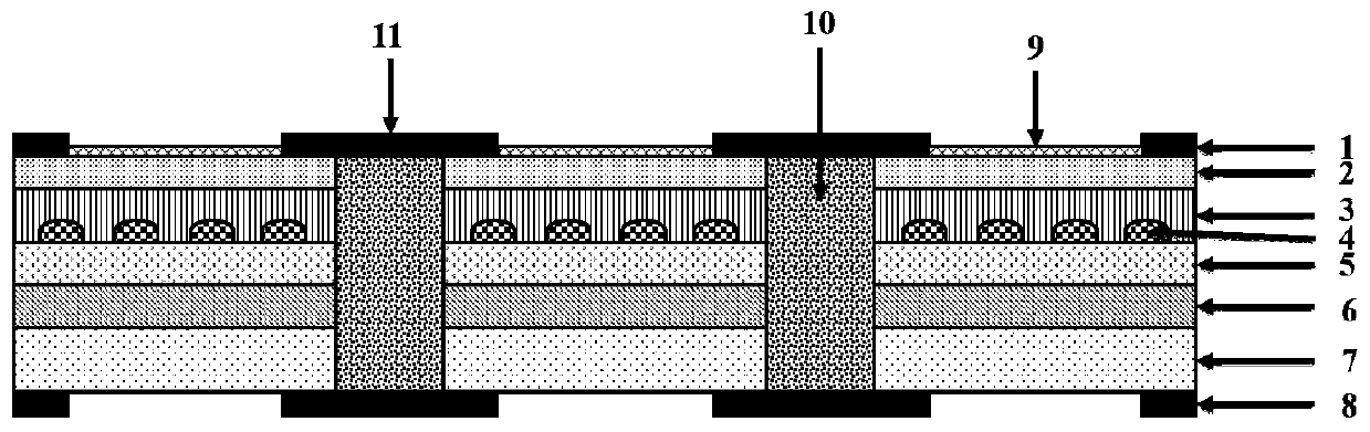
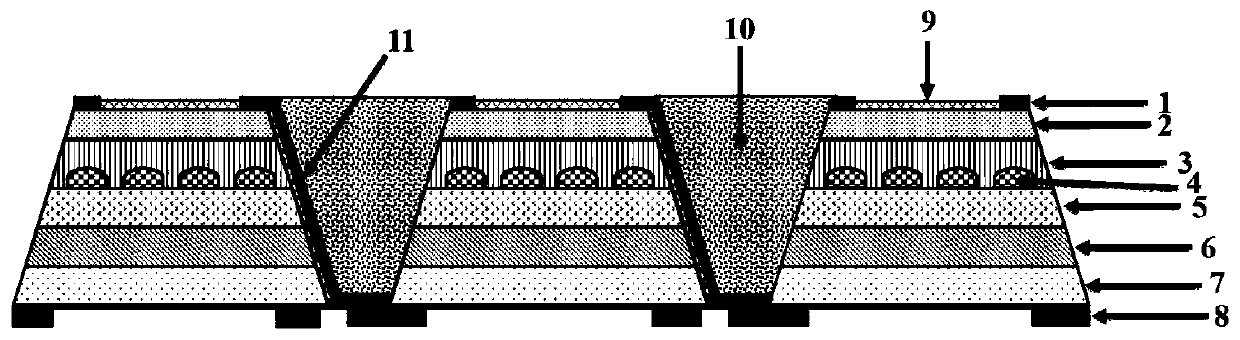
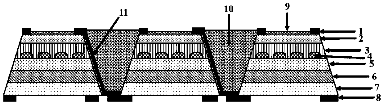
[0059] DETAILED DESCRIPTION OF THE PREFERRED EMBODIMENT 1. This embodiment is described with reference to FIG. 1 to FIG. 5 . The silicon detector array device with enhanced blue light efficiency provided by this embodiment includes a plurality of detection units, a plurality of isolation regions 10 and a plurality of electrode leads 11 .

[0060] Among them, a plurality of detection units are regularly arranged to form an array, and each detection unit includes an anode 1, a non-depletion layer 2, an absorption layer 3, a field control layer 5, an avalanche layer 6, a substrate layer 7, a cathode 8 and a light-transmitting layer 9. The field control layer 5 , the absorption layer 3 and the non-depletion layer 2 are sequentially arranged on the upper surface of the avalanche layer 6 from bottom to top. A doped junction 4 is provided inside the absorption layer 3 , the lower surface of the doped junction 4 is in contact with the upper surface of the field control layer 5 , and t...

specific Embodiment approach 2

[0067] Specific embodiment 2. For the parallel electrode structure array device, and the light-transmitting layer 9 and the anode 1 are all located on the same plane, the combination Image 6 To illustrate the present embodiment, the basic process steps are as follows:

[0068] Step 1. Select a highly doped n+ type silicon wafer as the substrate material of the array device, and perform cleaning treatment; the impurities are pentavalent elements such as P and As.

[0069] Step 2. Deposit a silicon epitaxial layer on the substrate material by techniques such as vapor phase epitaxy (VPE) or molecular beam epitaxy (MBE), as the p+ type avalanche layer 6 of the array device; the grown epitaxial material has low doping concentration and low defect of silicon.

[0070] Step 3: growing a p+-type Si-based field control layer 5 on the avalanche layer 6 by vapor phase epitaxy or molecular beam epitaxy.

[0071] Step 4: After the field control layer 5 is prepared, a p-type Si-based abs...

specific Embodiment approach 3

[0089] Specific embodiment 3. The manufacturing process for the situation where part of the lower surface of the light-transmitting layer 9 of the silicon detector array device for enhancing blue light efficiency is in contact with the non-depletion layer 2, and the remaining part is in contact with the upper surface of the anode 1: Step 14 and Step 15 in the specific embodiment 2 are combined and changed to: prepare an anti-reflection film with a thickness of about 0.1-5 μm on the upper surface of the non-depleted layer 2 and the anode 1 by low-temperature evaporation method as an array device The transparent layer 9.


PUM

PropertyMeasurementUnit
Thicknessaaaaaaaaaa
Thicknessaaaaaaaaaa
Thicknessaaaaaaaaaa

Abstract

A manufacturing method of a silicon detector array device for enhancing the blue light efficiency belongs to the field of photoelectric technology. The problem on how to provide a manufacturing methodof a silicon detector array device with high blue light sensitivity, high gain and high integration is solved. The preparation method of the invention includes the following steps: depositing an avalanche layer on a cleaned substrate material; depositing a field control layer on the upper surface of the avalanche layer; depositing an absorption layer on the upper surface of the field control layer and preparing doping junctions by ion implantation; depositing a non-depletion layer on the upper surface of the absorption layer; preparing isolation regions; preparing anodes and anode electrode leads; preparing a transparent layer on the non-depletion layer or on the non-depletion layer and the anodes; thinning the substrate; and finally, preparing cathodes and cathode electrode leads, removing the hard substrate, and completing packaging to obtain an array device. The array device manufactured by the method has high blue light responsiveness and high quantum efficiency.

Description

technical field [0001] The invention belongs to the field of optoelectronic technology, and in particular relates to a manufacturing method of a silicon detector array device for enhancing blue light efficiency. Background technique [0002] An avalanche photodiode (APD) is a photosensitive element commonly used in the field of optical communications. After a reverse bias is applied to the P-N junction of a photodiode made of silicon or germanium, the incident light will be absorbed by the P-N junction to form a photocurrent, and increasing the reverse bias will produce an "avalanche" ( That is, the photocurrent exponentially increases), this kind of diode is called "avalanche photodiode". [0003] The working principle of the avalanche photodiode is to use the directional movement of photo-generated carriers in a strong electric field to generate an avalanche effect to obtain the gain of photocurrent. In the avalanche process, the photogenerated carriers move in a high-sp...

Claims


Application Information

Patent Timeline
IPC IPC(8): H01L31/0224H01L31/0352H01L31/107H01L31/18
CPCH01L31/022408H01L31/022416H01L31/0352H01L31/107H01L31/18
Inventor 秦余欣王维彪梁静秋高丹陶金张军吕金光陈锋
Owner CHANGCHUN INST OF OPTICS FINE MECHANICS & PHYSICS CHINESE ACAD OF SCI
Why Eureka
Try Eureka