Thin-film transistor, display device, and preparation method of thin-film transistor

A technology of thin-film transistors and semiconductors, which is applied in the preparation of display devices and thin-film transistors. In the field of thin-film transistors, it can solve problems such as poor uniformity, restrictions on the application of large-size and flexible display devices, and difficult manufacturing processes, and achieve display performance improvement and driving. Effects of performance improvement and shutdown performance improvement

Pending Publication Date: 2019-05-10
YUNGU GUAN TECH CO LTD
View PDF5 Cites 1 Cited by
  • Summary
  • Abstract
  • Description
  • Claims
  • Application Information

AI Technical Summary

Problems solved by technology

The carrier mobility of low-temperature polysilicon thin-film transistors (LTPS TFT) is improved, but the manufacturing process is difficult and the uniformity is poor, which limits its application in large-size and flexible display devices

Method used


Image

  • Thin-film transistor, display device, and preparation method of thin-film transistor
  • Thin-film transistor, display device, and preparation method of thin-film transistor
  • Thin-film transistor, display device, and preparation method of thin-film transistor

Examples


Embodiment 1

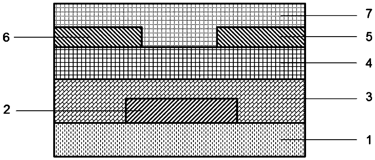
[0042] This embodiment provides a thin film transistor, such as figure 1 As shown, it includes: a gate electrode 2 formed on the substrate 1, an insulating layer 3 formed on the gate electrode 2 and extending to cover the top surface of the substrate 1, an active layer 4 formed on the insulating layer 3, and an active layer formed on the active layer The source electrode 6 and the drain electrode 5 on the source layer 4 are formed on the source and drain electrodes and partially cover the passivation layer 7 on the top surface of the active layer 4 .

[0043] The gate electrode 2 is made of metal molybdenum (Mo) doped with B + Forming, through ion doping, the gate electrode 2 is conductorized to increase the conductivity of the gate electrode 2 . The material of the insulating layer 3 is silicon oxide (SiOx), and the material of the source electrode 6 and the drain electrode 5 is titanium-aluminum-titanium lamination. The active layer 4 is an indium gallium zinc oxide film, ...

Embodiment 2

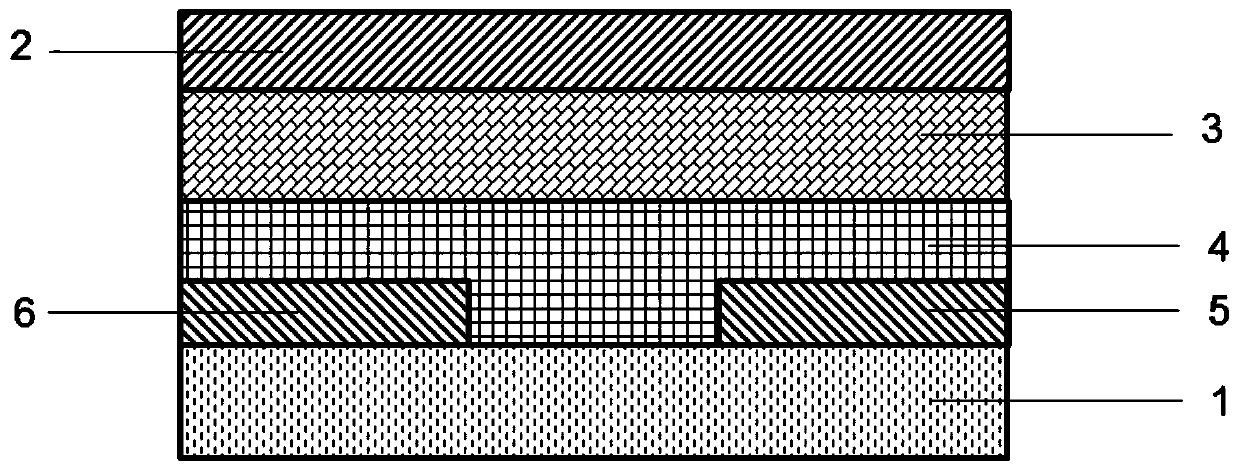
[0066] This embodiment provides a thin film transistor, which differs from the thin film transistor provided in Embodiment 1 in that: figure 2 As shown, the thin film transistor includes a gate electrode 2 formed on a substrate 1, an insulating layer 3 formed on the gate electrode 2 and extending to cover the top surface of the substrate 1, an active layer 4 formed on the insulating layer 3, and an active layer 4 formed on the active layer. A source electrode 6 and a drain electrode 5 on the layer 4 , a passivation layer 7 formed on the source and drain electrodes and partially covering the top surface of the active layer 4 .

[0067] Wherein, the active layer 4 is an indium gallium zinc oxide film, and the indium gallium zinc oxide film is doped with acetylacetone as a photosensitive active agent. The molar ratio of indium atoms: gallium atoms: zinc atoms: acetylacetone in the indium gallium zinc oxide film is 2:10:10:50.

[0068] The preparation method of the above-mention...

Embodiment 3

[0074] This embodiment provides a thin film transistor, which differs from the thin film transistor provided in Embodiment 1 in that in the thin film transistor as the active layer 4, the molar ratio of indium atoms: gallium atoms: zinc atoms: acetylacetone is 8:3 :3:5.

[0075] The difference between the preparation method of the above thin film transistor and the preparation method provided in Example 1 is that in step S32, In 3+ : Ga 3+ : Zn 2+ : The molar ratio of acetylacetone is 8:3:3:5, wherein, In 3+ The molar concentration is 10M.


PUM


Abstract

The invention discloses a thin-film transistor; an active layer of the thin-film transistor is an indium-gallium-zinc oxide film, and a photosensitive active agent is doped into the indium-gallium-zinc oxide film. By adopting the photosensitive active agent, the turn-off performance of the thin-film transistor is improved, an off-state current (Ioff) of the thin-film transistor is reduced, and a specific value of an on-state current and the off-state current of the thin-film transistor is increased (Ion / Ioff), and the driving performance of the thin-film transistor is improved. The invention discloses a preparation method of the thin-film transistor, the preparation method comprises the following steps: preparing the active layer, dissolving the photosensitive active agent in a first preparation solution to form a precursor solution, distributing the precursor solution on a base and curing to form the indium-gallium-zinc oxide film containing the photosensitive active agent. Through the preparation method disclosed by the invention, the use of the photoresist can be avoided, the preparation process of the active layer is simplified, and the damage of the active layer caused by stripping the photoresist can be avoided.

Description

technical field [0001] The invention belongs to the technical field of semiconductors, and in particular relates to a thin film transistor, a display device and a preparation method of the thin film transistor. Background technique [0002] A thin film transistor (Thin Film Transistor, TFT) is a field effect transistor, including source and drain electrodes, an active layer (also known as a channel layer), a gate electrode and an insulating layer (also known as a dielectric layer). As the core driving element of active matrix electronic devices, thin film transistors are widely used in active organic light-emitting diode displays and liquid crystal displays. [0003] Hydrogen-containing amorphous silicon thin-film transistors (a-Si:H TFTs) dominate active-matrix liquid crystal display (AM-LCD) devices, but a-Si:H TFTs have low carrier mobility and cannot drive size Larger AM-OLEDs. Polysilicon thin film transistors (p-Si TFTs) have high carrier mobility, but they need to b...

Claims


Application Information

Patent Timeline
IPC IPC(8): H01L29/786H01L21/34
Inventor 张峰李阳于锋杨海涛马应海刘晓佳
Owner YUNGU GUAN TECH CO LTD
Why Eureka
Try Eureka