Doped-free l-shaped tunneling field-effect transistor and its preparation method

A tunneling field effect, non-doped technology, used in semiconductor/solid-state device manufacturing, semiconductor devices, electrical components, etc., can solve the problems of increasing device static power consumption, device damage, high cost, etc., and achieve a simple manufacturing process. Ease of implementation, suppression of bipolar effects, and reduction of implementation costs

Active Publication Date: 2020-10-09
XIDIAN UNIV
View PDF5 Cites 0 Cited by
  • Summary
  • Abstract
  • Description
  • Claims
  • Application Information

AI Technical Summary

Problems solved by technology

Such a process will inevitably cause damage to the device, resulting in a higher concentration of traps
The existence of traps will degrade the sub-threshold swing and off-state current of the device, thereby reducing the switching speed of the device and increasing the static power consumption of the device, resulting in high cost of device preparation and limiting the application of the device

Method used


Image

  • Doped-free l-shaped tunneling field-effect transistor and its preparation method
  • Doped-free l-shaped tunneling field-effect transistor and its preparation method
  • Doped-free l-shaped tunneling field-effect transistor and its preparation method

Examples


Embodiment 1

[0034] Embodiment 1, manufacturing an undoped L-shaped tunneling field effect transistor whose gate is gallium metal with a work function of 4.2eV.

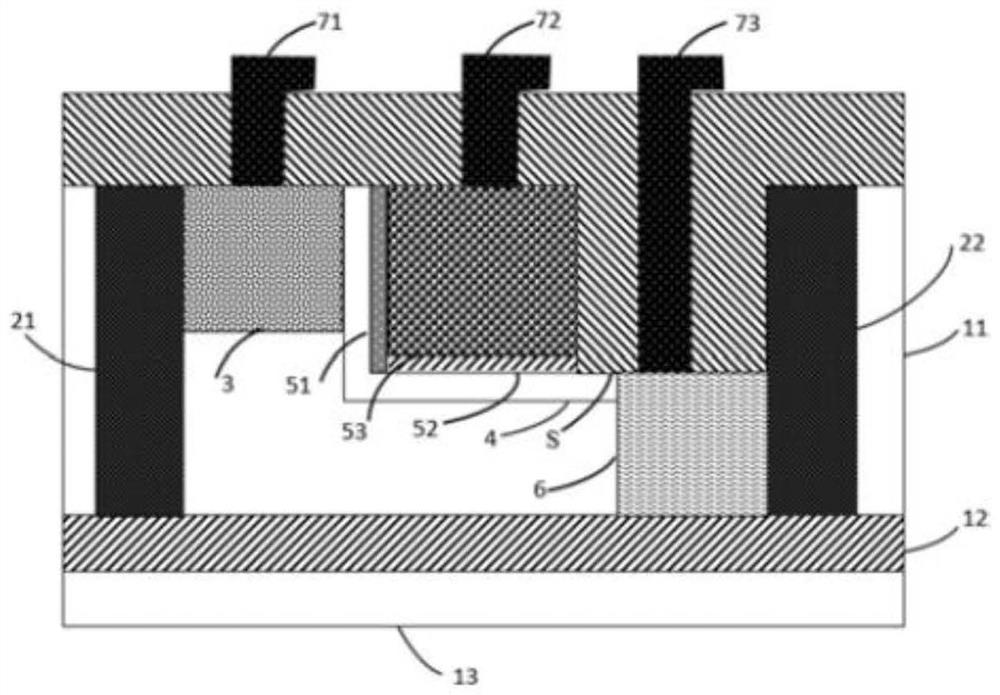
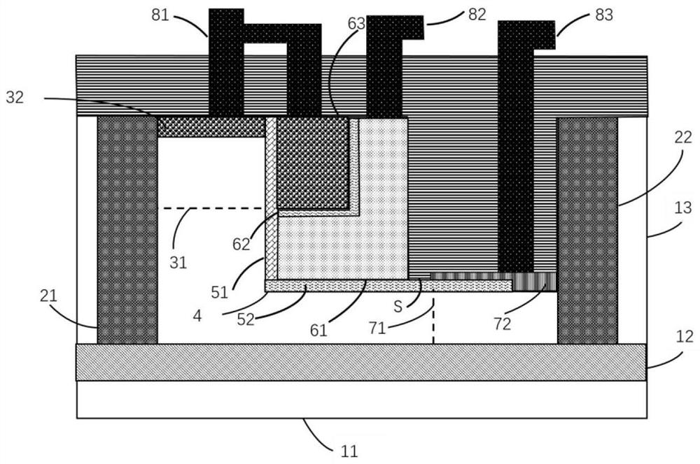
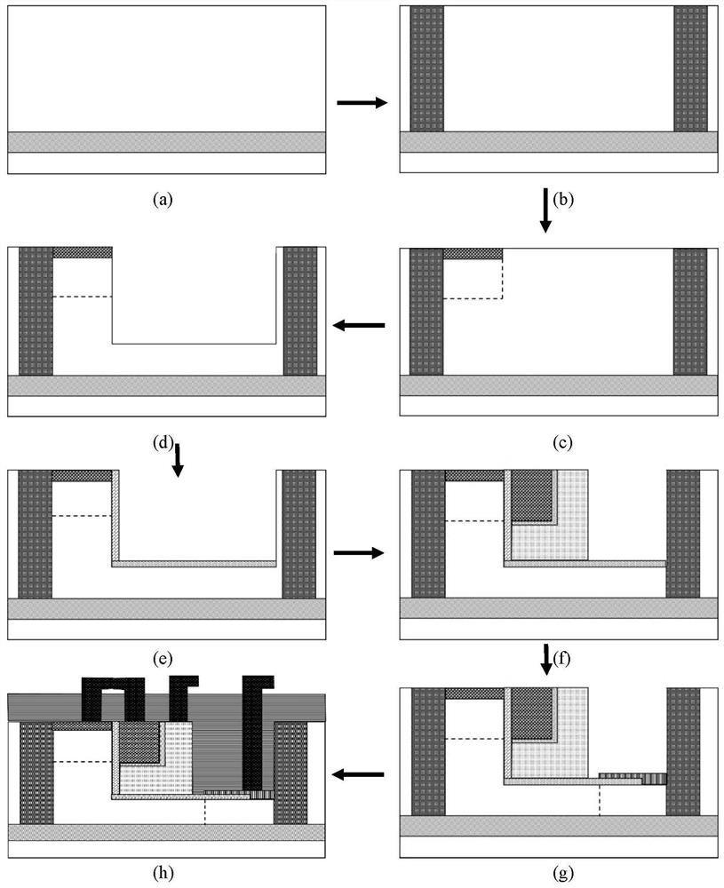
[0035] Step 1, make SOI substrate, such as image 3 (a).

[0036] 1a) Dry oxygen oxidation on the prepared bottom initial silicon wafer to generate SiO with a thickness of 10nm 2 Oxide buried layer;

[0037] 1b) Growing silicon with a thickness of 15 nm on the buried oxide layer as an epitaxial layer by an epitaxial growth process to form an SOI substrate.

[0038] Step 2, etching on both sides of the epitaxial silicon to form isolation grooves, such as image 3 (b).

[0039] 2a) Deposit SiO with a thickness of 2nm on the surface of epitaxial silicon 2 As a bottom oxide layer, then deposit Si with a thickness of 15nm on the surface of the layer 3 N 4 as a protective layer;

[0040] 2b) Using a photolithography machine, using a photolithography process on Si 3 N 4 A shallow trench isolation pattern is formed on the prote...

Embodiment 2

[0078] Embodiment 2, manufacturing an undoped L-shaped tunneling field effect transistor whose gate is tungsten metal with a work function of 4.5eV.

[0079] Step 1, making SOI substrate, such as image 3 (a).

[0080] 1.1) Dry oxygen oxidation on the prepared bottom initial silicon wafer to generate SiO with a thickness of 13nm 2 Oxide buried layer;

[0081] 1.2) An SOI substrate is formed by growing silicon with a thickness of 14 nm on the buried oxide layer as an epitaxial layer through an epitaxial growth process.

[0082] Step 2, etching on both sides of the epitaxial silicon to form isolation grooves, such as image 3 (b).

[0083] 2.1) Deposit SiO with a thickness of 4nm on the surface of epitaxial silicon 2 As a bottom oxide layer, then deposit Si with a thickness of 12nm on the surface of the layer 3 N 4 as a protective layer;

[0084] 2.2) Using a photolithography machine, using a photolithography process on Si 3 N 4 A shallow trench isolation pattern is fo...

Embodiment 3

[0122] Embodiment 3, manufacturing an undoped L-shaped tunneling field effect transistor whose gate is copper metal with a work function of 4.7eV.

[0123] The first step is to make the SOI substrate, such as image 3 (a).

[0124] First, dry oxygen oxidation is performed on the prepared bottom initial silicon wafer to produce SiO with a thickness of 15nm 2 An oxide buried layer; and then grow silicon with a thickness of 13nm on the oxide buried layer as an epitaxial layer through an epitaxial growth process to form an SOI substrate.

[0125] The second step is to etch and form isolation grooves on both sides of the epitaxial silicon, such as image 3 (b).

[0126] First, deposit SiO with a thickness of 5 nm on the surface of epitaxial silicon 2 As a bottom oxide layer, then deposit Si with a thickness of 10nm on the surface of the layer 3 N 4 As a protective layer; then use a photolithography machine, using photolithography process on Si 3 N 4 Form a shallow trench is...


PUM

PropertyMeasurementUnit
electron work functionaaaaaaaaaa

Abstract

The invention discloses an un-doped L-shaped tunneling field effect transistor and a preparation method thereof, which mainly solve the problems of large off-state current, serious bipolar effects andhigh preparation cost of the existing device. The un-doped L-shaped tunneling field effect transistor comprises an SOI substrate (1), a heterogeneous gate dielectric layer (5), a metal layer (6) anda conductive layer (8), wherein two sides of the SOI substrate are provided with isolation grooves (2); the upper surface of the SOI substrate is provided with a source region (3), a channel region (4) and a drain region (7); the heterogeneous gate dielectric layer and the metal layer are located at the upper side of the channel region; the source region, the channel region and the drain region are all made of un-doped intrinsic materials; the gate dielectric layer adopts a heterogeneous gate dielectric material, one side close to the source region adopts a high-K dielectric material and one side close to the drain region adopts a low-K dielectric material; and the metal layer is divided to an upper layer and a lower layer with different work functions, and the two metal layers are isolated by silicon dioxide. The off-state current is reduced, the bipolar effects are suppressed, the preparation cost is saved, and the un-doped L-shaped tunneling field effect transistor can be applied topreparation of a large-scale integrated circuit.

Description

technical field [0001] The invention belongs to the technical field of semiconductor devices, in particular to an L-shaped tunneling field-effect transistor, which is suitable for the manufacture of large-scale integrated circuits. Background technique [0002] Under the impetus of "Moore's Law", semiconductor integrated circuit technology develops rapidly and enters the nanometer dimension. However, as the size shrinks, the existence of short channel effects, parasitic effects and traps makes the performance of traditional MOSFETs seriously degrade when the size shrinks, which cannot meet the requirements of integrated circuit development. [0003] The Tunneling Field Effect Transistor (TFET) works on the basis of the band-to-band tunneling quantum tunneling effect mechanism, which theoretically breaks through the limit value of 60mV / decade of the subthreshold swing of the traditional MOSFET at room temperature. Therefore, TFET devices have fast switching characteristics a...

Claims


Application Information

Patent Timeline
Patent Type & Authority Patents(China)
IPC IPC(8): H01L29/423H01L29/49H01L29/51H01L29/10H01L29/16H01L29/739H01L21/28H01L21/331
Inventor 李聪郭嘉敏庄奕琪闫志蕊刘伟峰李振荣汤华莲
Owner XIDIAN UNIV
Why Eureka
Try Eureka