Semimetal/semiconductor Schottky junction, method for fabricating same, and Schottky diode

A Schottky diode and Schottky junction technology, applied in semiconductor/solid-state device manufacturing, diodes, semiconductor devices, etc., can solve the problems of interface diffusion and interface reaction, easy formation of defects, poor thermal stability, etc.

Active Publication Date: 2019-07-05
NANJING UNIV
View PDF4 Cites 1 Cited by
  • Summary
  • Abstract
  • Description
  • Claims
  • Application Information

AI Technical Summary

Problems solved by technology

Due to the difference in the properties of traditional metal and semiconductor materials, the thermal stability of the metal and semicondu

Method used


Image

  • Semimetal/semiconductor Schottky junction, method for fabricating same, and Schottky diode
  • Semimetal/semiconductor Schottky junction, method for fabricating same, and Schottky diode
  • Semimetal/semiconductor Schottky junction, method for fabricating same, and Schottky diode

Examples


preparation example Construction

[0043] In the present invention, the preparation method of the Schottky diode preferably comprises the following steps:

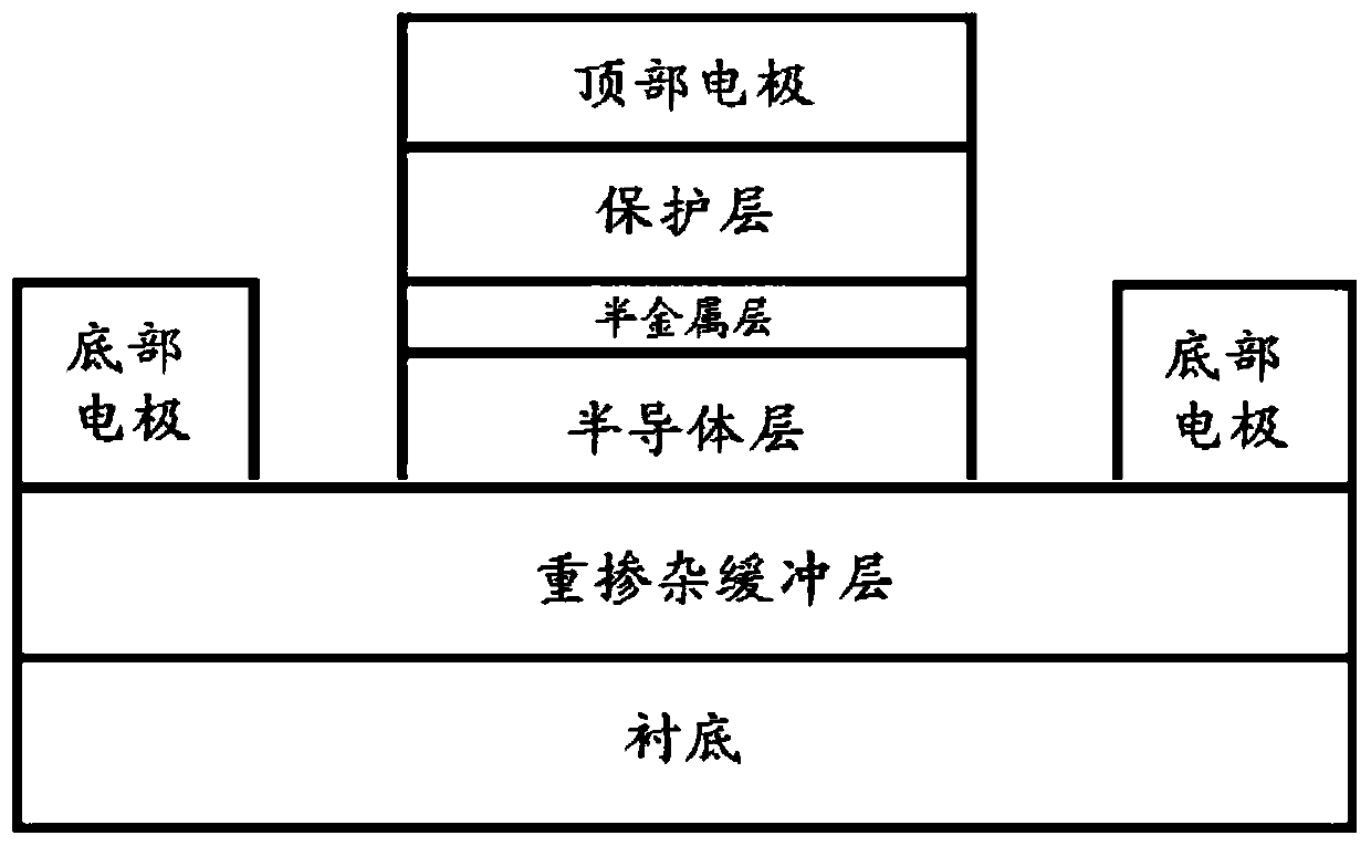
[0044] A material containing a heavily doped buffer layer, a semiconductor layer, a semi-metal layer and a protective layer is prepared on a substrate by molecular beam epitaxy, wherein the semi-metal / semiconductor Schottky junction formed by the semiconductor layer and the semi-metal layer For the half-metal / semiconductor Schottky junction of the above technical solution, an ohmic contact is formed between the protective layer and the half-metal layer; the position of the electrode is determined by photolithography, and the etching depth reaches the heavily doped buffer layer of the obtained material ; The top electrode is prepared on the protective layer by evaporation method; the bottom electrode is prepared on the etched heavily doped buffer layer to form a mesa structure, and an ohmic contact is formed between the bottom electrode and the heavily doped ...

Embodiment 1

[0052] (1) Deoxidize the GaAs substrate on the (001) crystal plane for 15 minutes. During the deoxidization process, the surface temperature of the GaAs substrate is 600°C;

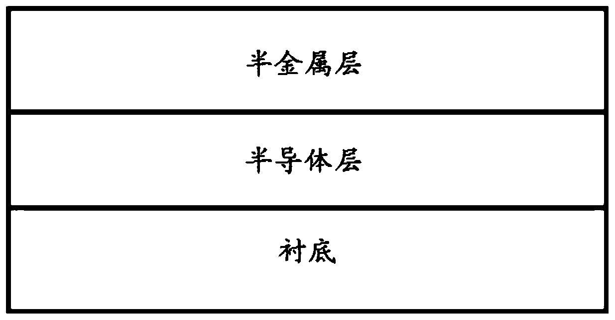
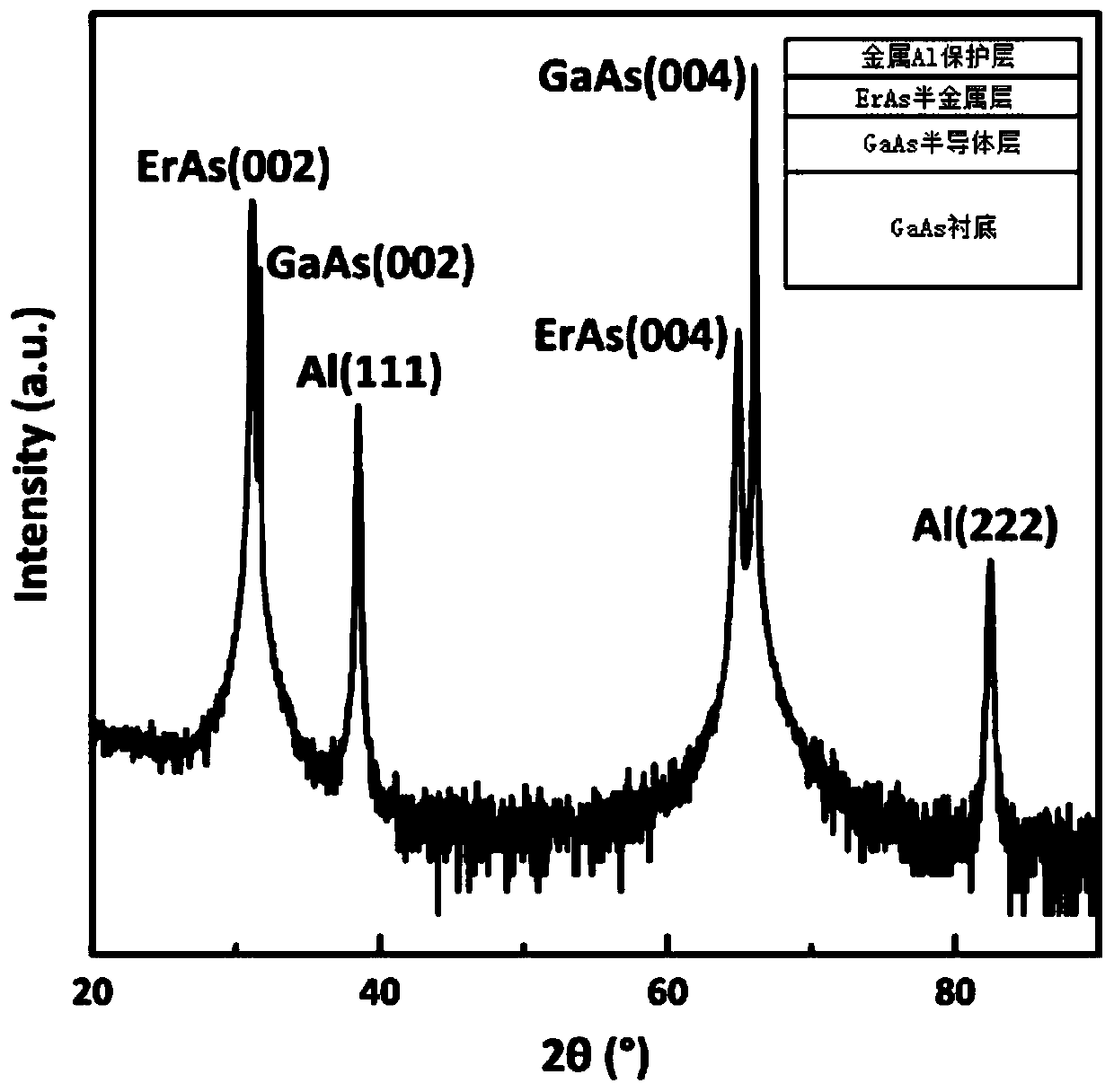
[0053] (2) Using the molecular beam epitaxy method, the background vacuum is 1×10 -7 ~1×10 -8 Epitaxial growth of a GaAs semiconductor layer (non-doped semiconductor layer, that is, no dopant source) on a GaAs substrate under torr and 580°C, with a thickness of 100 nm and a growth rate of 1 μm / h;

[0054] (3) Reduce the temperature of the obtained material to 455°C at a cooling rate of 30°C / min, and the background vacuum is 1×10 -7 ~1×10 -8 Under torr conditions, an ErAs semi-metal layer is epitaxially grown on the GaAs semiconductor layer by molecular beam epitaxy, with a thickness of 125 nm and a growth rate of 170 nm / h;

[0055] (4) Reduce the temperature of the obtained material to 50°C at a cooling rate of 30°C / min, and the background vacuum is 5×10 -10 When the Torr is lower than that, a metal A...

Embodiment 2

[0059] (1) After deoxidizing the GaAs substrate on the (001) crystal plane (the surface temperature of the GaAs substrate is 600°C, and the processing time is 15 minutes), molecular beam epitaxy is used in a background vacuum of 1×10 -7 ~1×10 -8 Under the conditions of torr and 580°C, taking the GaAs substrate as the reference, the GaAs heavily doped buffer layer (thickness: 100nm) and GaAs concentration gradient layer (thickness: 300nm) were epitaxially grown sequentially, the growth rate was 1μm / h, and the dopant source was Si, the content of the dopant source in the GaAs heavily doped buffer layer is 1×10 18 cm -3 , the content of the dopant source in the GaAs concentration gradient layer is 5×10 17 cm -3 ;

[0060] (2) Using the molecular beam epitaxy method, the background vacuum is 1×10 -7 ~1×10 -8 Under the condition of torr and 580°C, epitaxially grow a GaAs semiconductor layer on the GaAs concentration gradient layer (it is a doped semiconductor layer, the dopin...


PUM


Abstract

The invention relates to the field of electronic materials, and in particular to a semimetal/semiconductor Schottky junction, a method for fabricating the same, and a Schottky diode. The semimetal/semiconductor Schottky junction comprises a semiconductor layer and a semimetal layer, wherein a Schottky contact is formed between the semiconductor layer and the semimetal layer; and a compound formingthe semimetal layer is a compound composed of a rare earth element and a group VA element. The semimetal/semiconductor Schottky junction has good thermal stability at an interface between the semiconductor layer and the semimetal layer. The Schottky diode based on the semimetal/semiconductor Schottky junction has an ideal factor of about 1.05, noise equivalent power that can be reduced to the order of pW/Hz1/2 or even sub-pW/Hz1/2, and sensitive detection performance.

Description

technical field [0001] The invention relates to the technical field of electronic materials, in particular to a half-metal / semiconductor Schottky junction, a preparation method thereof, and a Schottky diode. Background technique [0002] Schottky diodes are widely used in high-speed integrated circuits and microwave technology, and their nonlinear characteristics can be used in high-frequency detection and harmonic generation. Ideally, the current-voltage characteristics of a Schottky diode conforming to the thermionic emission theory are [0003] [0004] [0005] Among them, I s is the reverse saturation current, q is the amount of charge (-e for electrons, e for holes), V is the applied bias voltage on the Schottky junction, k is the Boltzmann constant, T is the temperature, and A is junction area, A * is the effective Richardson constant, Φ B is the Schottky barrier. [0006] In practical cases, considering other current formation mechanisms, such as recombina...

Claims


Application Information

Patent Timeline
IPC IPC(8): H01L29/47H01L21/285H01L29/872
CPCH01L29/475H01L21/28581H01L29/872H01L29/0657H01L29/20H01L29/66212
Inventor 芦红丁元丰张克冬
Owner NANJING UNIV
Why Eureka
Try Eureka